

Key Insights
The global Thick Film Photoresist market is poised for significant expansion, projected to reach an estimated market size of approximately $1.2 billion in 2025. This growth trajectory is underpinned by a robust Compound Annual Growth Rate (CAGR) of around 6.5% anticipated over the forecast period of 2025-2033. The primary drivers fueling this expansion are the escalating demand for advanced semiconductor packaging solutions, particularly Wafer-Level Packaging (WLP) and Flip Chip (FC) technologies, which rely heavily on the precise patterning capabilities of thick film photoresists. The continuous innovation in microelectronics and the increasing complexity of integrated circuits necessitate high-performance photoresists for intricate circuit designs. Furthermore, the burgeoning electronics industry in the Asia Pacific region, driven by its manufacturing prowess and increasing domestic consumption, is a significant contributor to market growth.
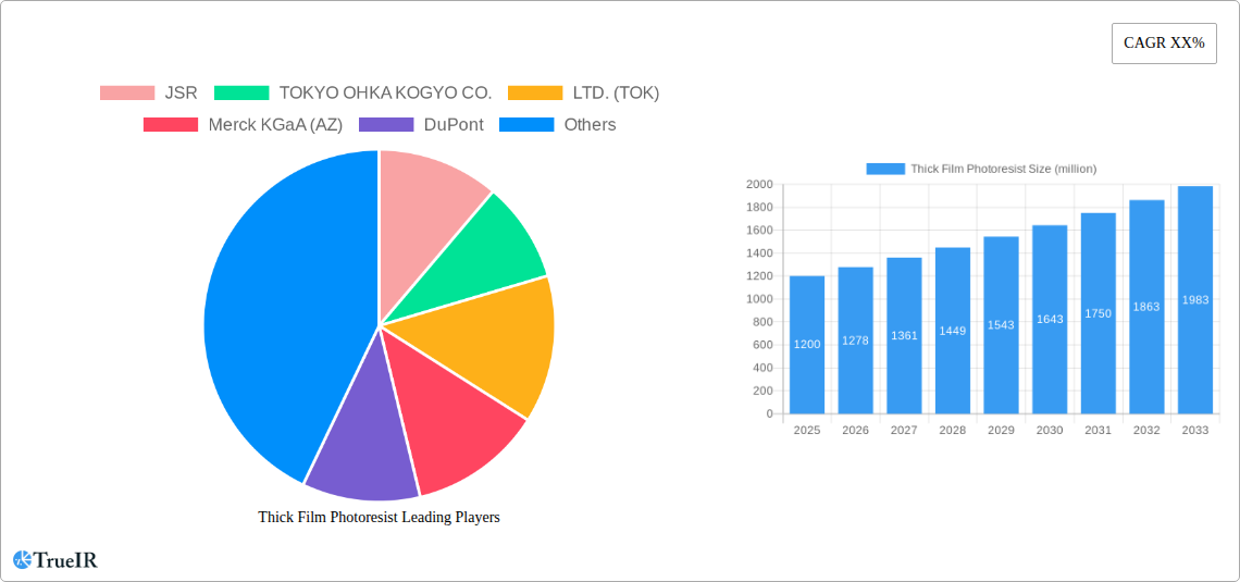
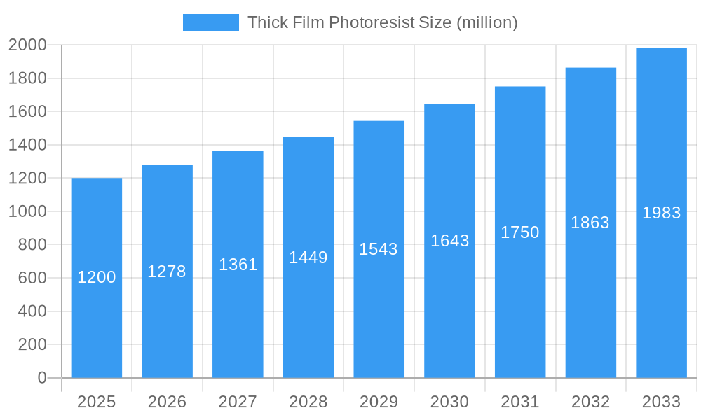
Thick Film Photoresist Market Size (In Billion)
Despite the optimistic outlook, certain restraints could temper the market's full potential. These include the high cost associated with research and development of novel photoresist formulations and the stringent regulatory requirements concerning environmental impact and safety standards, which can increase operational expenses for manufacturers. Additionally, the emergence of alternative lithography techniques and materials could pose a competitive challenge. However, the inherent advantages of thick film photoresists, such as their versatility in handling thicker films required for various applications and their established reliability in high-volume manufacturing, are expected to sustain their market relevance. The market is segmented into Thick Film Positive Photoresists and Thick Film Negative Photoresists, with both types witnessing steady demand across diverse applications, including advanced semiconductor packaging, MEMS fabrication, and display manufacturing. Leading companies such as JSR, TOYO OHKA KOGYO (TOK), and Merck KGaA are at the forefront of innovation, continuously developing advanced formulations to meet the evolving needs of the electronics industry.
Thick Film Photoresist Company Market Share
This in-depth report provides a dynamic and SEO-optimized analysis of the global Thick Film Photoresist market. Leveraging high-volume keywords essential for industry professionals, this study delves into market structure, trends, competitive landscape, dominant segments, and future outlook. Covering a comprehensive study period from 2019 to 2033, with a base year of 2025 and a forecast period extending to 2033, this report offers unparalleled insights for stakeholders seeking to navigate and capitalize on this critical sector of the electronics manufacturing industry.
Thick Film Photoresist Market Structure & Competitive Landscape
The thick film photoresist market exhibits a moderately concentrated structure, driven by intense innovation and significant R&D investments. Leading players like JSR, TOKYO OHKA KOGYO CO.,LTD. (TOK), and Merck KGaA (AZ) command substantial market share due to their advanced technological capabilities and extensive product portfolios. DuPont and Shin-Etsu are also key contenders, contributing to the competitive intensity through ongoing product development and strategic partnerships. The market's innovation drivers are primarily centered around enhancing resolution, improving process efficiency, and developing more environmentally friendly formulations. Regulatory impacts, particularly concerning chemical safety and waste management, are increasingly shaping market dynamics, pushing for sustainable alternatives. Product substitutes, while present in niche applications, face challenges in matching the performance and cost-effectiveness of established thick film photoresists. End-user segmentation reveals a strong reliance on the semiconductor and electronics industries, with wafer-level packaging and flip-chip applications representing major growth avenues. Merger and acquisition (M&A) trends, although not consistently high in volume, are strategically important for consolidating market presence and acquiring complementary technologies. The current M&A activity is estimated to be in the range of one to three significant deals annually, primarily focused on specialized technology acquisitions.
- Market Concentration: Moderately concentrated with key players holding significant shares.
- Innovation Drivers: Resolution enhancement, process efficiency, sustainability.
- Regulatory Impacts: Increasing focus on environmental compliance and safety standards.
- Product Substitutes: Limited in core applications due to performance and cost barriers.
- End-User Segmentation: Dominance of semiconductor and electronics manufacturing.
- M&A Trends: Strategic acquisitions for technology and market expansion.
Thick Film Photoresist Market Trends & Opportunities
The global thick film photoresist market is projected for substantial growth, driven by the burgeoning demand for advanced electronic devices and components. The market size is estimated to reach $5,000 million by 2025 and is expected to expand to $8,000 million by 2033, exhibiting a Compound Annual Growth Rate (CAGR) of approximately 6.0% during the forecast period of 2025–2033. This robust expansion is underpinned by several key technological shifts and evolving consumer preferences. The relentless miniaturization of electronic devices, coupled with the increasing complexity of integrated circuits, necessitates the use of high-performance photoresists capable of achieving finer feature sizes and superior pattern definition. Wafer-level packaging and flip-chip technologies, crucial for enhancing device performance and reliability, are experiencing significant adoption, thereby fueling the demand for specialized thick film photoresists.
Consumer preferences are increasingly leaning towards smaller, more powerful, and energy-efficient electronic gadgets, ranging from smartphones and wearables to advanced automotive electronics and IoT devices. This trend directly translates into a higher demand for sophisticated semiconductor manufacturing processes, where thick film photoresists play a pivotal role. The competitive dynamics within the market are characterized by continuous innovation, with companies investing heavily in R&D to develop next-generation photoresists with improved sensitivity, wider processing windows, and enhanced material properties. The market penetration rate for advanced thick film photoresists is steadily increasing across various segments of the electronics industry.
Emerging opportunities lie in the development of novel photoresist formulations that offer greater environmental sustainability, such as water-soluble or low-VOC (Volatile Organic Compound) options, to align with global environmental regulations and corporate sustainability goals. The expanding applications in areas like advanced display technologies, MEMS (Micro-Electro-Mechanical Systems), and printed electronics also present significant growth avenues. The report analyzes the market size growth from an estimated $4,500 million in the historical year of 2024 to an estimated $8,000 million by 2033, showcasing a significant upward trajectory. The CAGR for the entire forecast period is projected to be around 6.0%. Technological shifts include advancements in lithography techniques that require photoresists with specific optical and chemical properties, further driving innovation and market diversification. Consumer preferences for higher functionality and smaller form factors in electronic devices are a constant catalyst for the photoresist industry.
Dominant Markets & Segments in Thick Film Photoresist
The Thick Film Photoresist market is experiencing dominant growth in the Asia-Pacific region, particularly in countries like China, South Korea, and Taiwan, driven by their expansive semiconductor manufacturing infrastructure and significant investments in advanced electronics production. This region is estimated to account for over 60% of the global market share. Key growth drivers in this region include robust government policies supporting the semiconductor industry, the presence of major foundries and packaging houses, and a rapidly growing domestic demand for electronic devices.
Within the application segmentation, Wafer-Level Packaging emerges as the most dominant segment, projected to consume a substantial portion of thick film photoresists, estimated at $3,000 million in 2025. This dominance is attributed to the increasing trend of advanced packaging techniques that enable smaller, more powerful, and cost-effective electronic components. Flip Chip (FC) technology, another critical application, is also experiencing significant expansion, with an estimated market value of $2,000 million in 2025, driven by its advantages in high-density interconnects and thermal management for high-performance processors. The "Others" segment, encompassing applications in MEMS, printed electronics, and advanced displays, is also showing promising growth, albeit from a smaller base.
In terms of product types, Thick Film Positive Photoresists are currently leading the market, with an estimated value of $3,500 million in 2025. This is due to their superior resolution capabilities, making them ideal for intricate patterning in advanced semiconductor fabrication. Thick Film Negative Photoresists, while also important, are projected to hold a significant share of $1,500 million in 2025, catering to specific applications where their chemical properties offer advantages. Key growth drivers for positive photoresists include the increasing demand for high-resolution lithography in leading-edge semiconductor nodes. For negative photoresists, growth is propelled by applications requiring robust chemical resistance and excellent adhesion. The continuous advancements in lithography equipment and processes, such as Extreme Ultraviolet (EUV) lithography, are also creating new opportunities and demands for specialized photoresist formulations, further solidifying the dominance of advanced positive photoresists in high-end applications.
Thick Film Photoresist Product Analysis
Product innovation in the thick film photoresist market is primarily focused on enhancing resolution, improving processing speed, and achieving greater environmental sustainability. Key advancements include the development of lower-viscosity formulations for finer feature patterning in wafer-level packaging and flip-chip applications. Companies are also introducing photoresists with enhanced thermal stability and chemical resistance to withstand demanding fabrication processes. The competitive advantage lies in offering tailored solutions that meet the specific requirements of advanced semiconductor nodes and emerging electronic technologies. The market fit is driven by the direct correlation between photoresist performance and the miniaturization and efficiency of electronic components, making product development a crucial differentiator.
Key Drivers, Barriers & Challenges in Thick Film Photoresist
The thick film photoresist market is propelled by several key drivers, including the relentless demand for miniaturization and increased performance in electronic devices, the rapid growth of the semiconductor industry, and the expanding applications in wafer-level packaging and flip-chip technologies. Technological advancements in lithography techniques further stimulate the need for more sophisticated photoresist materials. Government initiatives supporting domestic semiconductor manufacturing also play a significant role.
However, the market faces significant barriers and challenges. Supply chain disruptions, as witnessed in recent years, can impact raw material availability and pricing, leading to production delays and increased costs. Stringent and evolving environmental regulations concerning chemical usage and waste disposal pose compliance hurdles and necessitate investment in greener formulations. Intense competition among established players and emerging market entrants drives down profit margins and demands continuous innovation. The high cost of R&D and the capital-intensive nature of photoresist manufacturing also present financial challenges for smaller companies.
Growth Drivers in the Thick Film Photoresist Market
The growth of the thick film photoresist market is primarily fueled by the accelerating demand for advanced semiconductor devices across various sectors, including consumer electronics, automotive, and telecommunications. The ongoing miniaturization trend, pushing for smaller and more powerful chips, directly translates into a higher requirement for high-resolution photoresists. Furthermore, the increasing adoption of advanced packaging techniques like wafer-level packaging and flip-chip assembly for enhanced device performance and reliability is a significant growth catalyst. Government support and incentives for the semiconductor industry in key regions, coupled with the expansion of 5G infrastructure and the proliferation of IoT devices, are also creating substantial market opportunities and driving consistent demand for innovative thick film photoresist solutions.
Challenges Impacting Thick Film Photoresist Growth
Despite robust growth potential, the thick film photoresist market faces several critical challenges. Evolving and stringent environmental regulations globally necessitate continuous investment in developing eco-friendly formulations and sustainable manufacturing processes, adding to operational costs and R&D expenditures. Supply chain volatility, particularly concerning the availability and pricing of key raw materials, poses a significant risk to production timelines and cost management. The highly competitive landscape, characterized by intense price pressures and the need for constant technological innovation, requires substantial capital investment and can hinder profitability for less established players. Furthermore, the specialized nature of photoresist applications demands continuous adaptation to the rapid pace of technological advancements in lithography and semiconductor manufacturing, requiring significant R&D resources and expertise.
Key Players Shaping the Thick Film Photoresist Market
- JSR
- TOKYO OHKA KOGYO CO.,LTD. (TOK)
- Merck KGaA (AZ)
- DuPont
- Shin-Etsu
- Allresist
- Futurrex
- KemLab™ Inc
- Youngchang Chemical
- Everlight Chemical
- Crystal Clear Electronic Material
- Kempur Microelectronics Inc
- Xuzhou B & C Chemical
Significant Thick Film Photoresist Industry Milestones
- 2019: Launch of advanced positive photoresists with enhanced resolution for sub-10nm semiconductor nodes.
- 2020: Increased focus on developing environmentally friendly, lower-VOC photoresist formulations due to growing regulatory pressures.
- 2021: Significant M&A activity as larger players acquire specialized photoresist technology firms to strengthen their portfolios, with an estimated three major acquisitions.
- 2022: Introduction of new negative photoresists optimized for thick film applications in advanced packaging, offering improved adhesion and chemical resistance.
- 2023: Expansion of production capacities by key players in Asia-Pacific to meet the surging demand for semiconductor manufacturing materials.
- 2024: Introduction of novel photoresist formulations designed for emerging applications like flexible electronics and micro-LED displays.
Future Outlook for Thick Film Photoresist Market
The future outlook for the thick film photoresist market remains exceptionally bright, driven by the accelerating pace of technological innovation in the semiconductor and electronics industries. The persistent demand for higher performance, increased functionality, and miniaturization in electronic devices will continue to be the primary growth catalyst. Emerging opportunities in advanced packaging, the expansion of IoT ecosystems, the evolution of automotive electronics, and the deployment of next-generation communication technologies like 6G will fuel sustained demand for high-quality, specialized thick film photoresists. Strategic collaborations, focused R&D on sustainable and high-performance materials, and expansion into new application areas will be key to capitalizing on the significant market potential estimated to reach $8,000 million by 2033.
Thick Film Photoresist Segmentation
-
1. Application
- 1.1. Wafer-Level Packaging
- 1.2. Flip Chip (FC)
- 1.3. Others
-
2. Types
- 2.1. Thick Film Positive Photoresists
- 2.2. Thick Film Negative Photoresists
Thick Film Photoresist Segmentation By Geography
-
1. North America
- 1.1. United States
- 1.2. Canada
- 1.3. Mexico
-
2. South America
- 2.1. Brazil
- 2.2. Argentina
- 2.3. Rest of South America
-
3. Europe
- 3.1. United Kingdom
- 3.2. Germany
- 3.3. France
- 3.4. Italy
- 3.5. Spain
- 3.6. Russia
- 3.7. Benelux
- 3.8. Nordics
- 3.9. Rest of Europe
-
4. Middle East & Africa
- 4.1. Turkey
- 4.2. Israel
- 4.3. GCC
- 4.4. North Africa
- 4.5. South Africa
- 4.6. Rest of Middle East & Africa
-
5. Asia Pacific
- 5.1. China
- 5.2. India
- 5.3. Japan
- 5.4. South Korea
- 5.5. ASEAN
- 5.6. Oceania
- 5.7. Rest of Asia Pacific
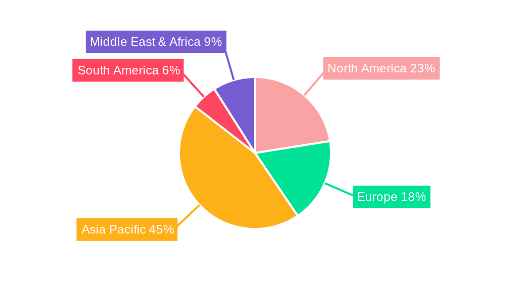
Thick Film Photoresist Regional Market Share
Geographic Coverage of Thick Film Photoresist
Thick Film Photoresist REPORT HIGHLIGHTS
| Aspects | Details |
|---|---|
| Study Period | 2020-2034 |
| Base Year | 2025 |
| Estimated Year | 2026 |
| Forecast Period | 2026-2034 |
| Historical Period | 2020-2025 |
| Growth Rate | CAGR of 7.8% from 2020-2034 |
| Segmentation |
|
Table of Contents
- 1. Introduction
- 1.1. Research Scope
- 1.2. Market Segmentation
- 1.3. Research Objective
- 1.4. Definitions and Assumptions
- 2. Executive Summary
- 2.1. Market Snapshot
- 3. Market Dynamics
- 3.1. Market Drivers
- 3.2. Market Restrains
- 3.3. Market Trends
- 3.4. Market Opportunities
- 4. Market Factor Analysis
- 4.1. Porters Five Forces
- 4.1.1. Bargaining Power of Suppliers
- 4.1.2. Bargaining Power of Buyers
- 4.1.3. Threat of New Entrants
- 4.1.4. Threat of Substitutes
- 4.1.5. Competitive Rivalry
- 4.2. PESTEL analysis
- 4.3. BCG Analysis
- 4.3.1. Stars (High Growth, High Market Share)
- 4.3.2. Cash Cows (Low Growth, High Market Share)
- 4.3.3. Question Mark (High Growth, Low Market Share)
- 4.3.4. Dogs (Low Growth, Low Market Share)
- 4.4. Ansoff Matrix Analysis
- 4.5. Supply Chain Analysis
- 4.6. Regulatory Landscape
- 4.7. Current Market Potential and Opportunity Assessment (TAM–SAM–SOM Framework)
- 4.8. TIR Analyst Note
- 4.1. Porters Five Forces
- 5. Market Analysis, Insights and Forecast 2021-2033
- 5.1. Market Analysis, Insights and Forecast - by Application
- 5.1.1. Wafer-Level Packaging
- 5.1.2. Flip Chip (FC)
- 5.1.3. Others
- 5.2. Market Analysis, Insights and Forecast - by Types
- 5.2.1. Thick Film Positive Photoresists
- 5.2.2. Thick Film Negative Photoresists
- 5.3. Market Analysis, Insights and Forecast - by Region
- 5.3.1. North America
- 5.3.2. South America
- 5.3.3. Europe
- 5.3.4. Middle East & Africa
- 5.3.5. Asia Pacific
- 5.1. Market Analysis, Insights and Forecast - by Application
- 6. Global Thick Film Photoresist Analysis, Insights and Forecast, 2021-2033
- 6.1. Market Analysis, Insights and Forecast - by Application
- 6.1.1. Wafer-Level Packaging
- 6.1.2. Flip Chip (FC)
- 6.1.3. Others
- 6.2. Market Analysis, Insights and Forecast - by Types
- 6.2.1. Thick Film Positive Photoresists
- 6.2.2. Thick Film Negative Photoresists
- 6.1. Market Analysis, Insights and Forecast - by Application
- 7. North America Thick Film Photoresist Analysis, Insights and Forecast, 2020-2032
- 7.1. Market Analysis, Insights and Forecast - by Application
- 7.1.1. Wafer-Level Packaging
- 7.1.2. Flip Chip (FC)
- 7.1.3. Others
- 7.2. Market Analysis, Insights and Forecast - by Types
- 7.2.1. Thick Film Positive Photoresists
- 7.2.2. Thick Film Negative Photoresists
- 7.1. Market Analysis, Insights and Forecast - by Application
- 8. South America Thick Film Photoresist Analysis, Insights and Forecast, 2020-2032
- 8.1. Market Analysis, Insights and Forecast - by Application
- 8.1.1. Wafer-Level Packaging
- 8.1.2. Flip Chip (FC)
- 8.1.3. Others
- 8.2. Market Analysis, Insights and Forecast - by Types
- 8.2.1. Thick Film Positive Photoresists
- 8.2.2. Thick Film Negative Photoresists
- 8.1. Market Analysis, Insights and Forecast - by Application
- 9. Europe Thick Film Photoresist Analysis, Insights and Forecast, 2020-2032
- 9.1. Market Analysis, Insights and Forecast - by Application
- 9.1.1. Wafer-Level Packaging
- 9.1.2. Flip Chip (FC)
- 9.1.3. Others
- 9.2. Market Analysis, Insights and Forecast - by Types
- 9.2.1. Thick Film Positive Photoresists
- 9.2.2. Thick Film Negative Photoresists
- 9.1. Market Analysis, Insights and Forecast - by Application
- 10. Middle East & Africa Thick Film Photoresist Analysis, Insights and Forecast, 2020-2032
- 10.1. Market Analysis, Insights and Forecast - by Application
- 10.1.1. Wafer-Level Packaging
- 10.1.2. Flip Chip (FC)
- 10.1.3. Others
- 10.2. Market Analysis, Insights and Forecast - by Types
- 10.2.1. Thick Film Positive Photoresists
- 10.2.2. Thick Film Negative Photoresists
- 10.1. Market Analysis, Insights and Forecast - by Application
- 11. Asia Pacific Thick Film Photoresist Analysis, Insights and Forecast, 2020-2032
- 11.1. Market Analysis, Insights and Forecast - by Application
- 11.1.1. Wafer-Level Packaging
- 11.1.2. Flip Chip (FC)
- 11.1.3. Others
- 11.2. Market Analysis, Insights and Forecast - by Types
- 11.2.1. Thick Film Positive Photoresists
- 11.2.2. Thick Film Negative Photoresists
- 11.1. Market Analysis, Insights and Forecast - by Application
- 12. Competitive Analysis
- 12.1. Company Profiles
- 12.1.1 JSR
- 12.1.1.1. Company Overview
- 12.1.1.2. Products
- 12.1.1.3. Company Financials
- 12.1.1.4. SWOT Analysis
- 12.1.2 TOKYO OHKA KOGYO CO.
- 12.1.2.1. Company Overview
- 12.1.2.2. Products
- 12.1.2.3. Company Financials
- 12.1.2.4. SWOT Analysis
- 12.1.3 LTD. (TOK)
- 12.1.3.1. Company Overview
- 12.1.3.2. Products
- 12.1.3.3. Company Financials
- 12.1.3.4. SWOT Analysis
- 12.1.4 Merck KGaA (AZ)
- 12.1.4.1. Company Overview
- 12.1.4.2. Products
- 12.1.4.3. Company Financials
- 12.1.4.4. SWOT Analysis
- 12.1.5 DuPont
- 12.1.5.1. Company Overview
- 12.1.5.2. Products
- 12.1.5.3. Company Financials
- 12.1.5.4. SWOT Analysis
- 12.1.6 Shin-Etsu
- 12.1.6.1. Company Overview
- 12.1.6.2. Products
- 12.1.6.3. Company Financials
- 12.1.6.4. SWOT Analysis
- 12.1.7 Allresist
- 12.1.7.1. Company Overview
- 12.1.7.2. Products
- 12.1.7.3. Company Financials
- 12.1.7.4. SWOT Analysis
- 12.1.8 Futurrex
- 12.1.8.1. Company Overview
- 12.1.8.2. Products
- 12.1.8.3. Company Financials
- 12.1.8.4. SWOT Analysis
- 12.1.9 KemLab™ Inc
- 12.1.9.1. Company Overview
- 12.1.9.2. Products
- 12.1.9.3. Company Financials
- 12.1.9.4. SWOT Analysis
- 12.1.10 Youngchang Chemical
- 12.1.10.1. Company Overview
- 12.1.10.2. Products
- 12.1.10.3. Company Financials
- 12.1.10.4. SWOT Analysis
- 12.1.11 Everlight Chemical
- 12.1.11.1. Company Overview
- 12.1.11.2. Products
- 12.1.11.3. Company Financials
- 12.1.11.4. SWOT Analysis
- 12.1.12 Crystal Clear Electronic Material
- 12.1.12.1. Company Overview
- 12.1.12.2. Products
- 12.1.12.3. Company Financials
- 12.1.12.4. SWOT Analysis
- 12.1.13 Kempur Microelectronics Inc
- 12.1.13.1. Company Overview
- 12.1.13.2. Products
- 12.1.13.3. Company Financials
- 12.1.13.4. SWOT Analysis
- 12.1.14 Xuzhou B & C Chemical
- 12.1.14.1. Company Overview
- 12.1.14.2. Products
- 12.1.14.3. Company Financials
- 12.1.14.4. SWOT Analysis
- 12.1.1 JSR
- 12.2. Market Entropy
- 12.2.1 Company's Key Areas Served
- 12.2.2 Recent Developments
- 12.3. Company Market Share Analysis 2025
- 12.3.1 Top 5 Companies Market Share Analysis
- 12.3.2 Top 3 Companies Market Share Analysis
- 12.4. List of Potential Customers
- 13. Research Methodology
List of Figures
- Figure 1: Global Thick Film Photoresist Revenue Breakdown (undefined, %) by Region 2025 & 2033
- Figure 2: Global Thick Film Photoresist Volume Breakdown (K, %) by Region 2025 & 2033
- Figure 3: North America Thick Film Photoresist Revenue (undefined), by Application 2025 & 2033
- Figure 4: North America Thick Film Photoresist Volume (K), by Application 2025 & 2033
- Figure 5: North America Thick Film Photoresist Revenue Share (%), by Application 2025 & 2033
- Figure 6: North America Thick Film Photoresist Volume Share (%), by Application 2025 & 2033
- Figure 7: North America Thick Film Photoresist Revenue (undefined), by Types 2025 & 2033
- Figure 8: North America Thick Film Photoresist Volume (K), by Types 2025 & 2033
- Figure 9: North America Thick Film Photoresist Revenue Share (%), by Types 2025 & 2033
- Figure 10: North America Thick Film Photoresist Volume Share (%), by Types 2025 & 2033
- Figure 11: North America Thick Film Photoresist Revenue (undefined), by Country 2025 & 2033
- Figure 12: North America Thick Film Photoresist Volume (K), by Country 2025 & 2033
- Figure 13: North America Thick Film Photoresist Revenue Share (%), by Country 2025 & 2033
- Figure 14: North America Thick Film Photoresist Volume Share (%), by Country 2025 & 2033
- Figure 15: South America Thick Film Photoresist Revenue (undefined), by Application 2025 & 2033
- Figure 16: South America Thick Film Photoresist Volume (K), by Application 2025 & 2033
- Figure 17: South America Thick Film Photoresist Revenue Share (%), by Application 2025 & 2033
- Figure 18: South America Thick Film Photoresist Volume Share (%), by Application 2025 & 2033
- Figure 19: South America Thick Film Photoresist Revenue (undefined), by Types 2025 & 2033
- Figure 20: South America Thick Film Photoresist Volume (K), by Types 2025 & 2033
- Figure 21: South America Thick Film Photoresist Revenue Share (%), by Types 2025 & 2033
- Figure 22: South America Thick Film Photoresist Volume Share (%), by Types 2025 & 2033
- Figure 23: South America Thick Film Photoresist Revenue (undefined), by Country 2025 & 2033
- Figure 24: South America Thick Film Photoresist Volume (K), by Country 2025 & 2033
- Figure 25: South America Thick Film Photoresist Revenue Share (%), by Country 2025 & 2033
- Figure 26: South America Thick Film Photoresist Volume Share (%), by Country 2025 & 2033
- Figure 27: Europe Thick Film Photoresist Revenue (undefined), by Application 2025 & 2033
- Figure 28: Europe Thick Film Photoresist Volume (K), by Application 2025 & 2033
- Figure 29: Europe Thick Film Photoresist Revenue Share (%), by Application 2025 & 2033
- Figure 30: Europe Thick Film Photoresist Volume Share (%), by Application 2025 & 2033
- Figure 31: Europe Thick Film Photoresist Revenue (undefined), by Types 2025 & 2033
- Figure 32: Europe Thick Film Photoresist Volume (K), by Types 2025 & 2033
- Figure 33: Europe Thick Film Photoresist Revenue Share (%), by Types 2025 & 2033
- Figure 34: Europe Thick Film Photoresist Volume Share (%), by Types 2025 & 2033
- Figure 35: Europe Thick Film Photoresist Revenue (undefined), by Country 2025 & 2033
- Figure 36: Europe Thick Film Photoresist Volume (K), by Country 2025 & 2033
- Figure 37: Europe Thick Film Photoresist Revenue Share (%), by Country 2025 & 2033
- Figure 38: Europe Thick Film Photoresist Volume Share (%), by Country 2025 & 2033
- Figure 39: Middle East & Africa Thick Film Photoresist Revenue (undefined), by Application 2025 & 2033
- Figure 40: Middle East & Africa Thick Film Photoresist Volume (K), by Application 2025 & 2033
- Figure 41: Middle East & Africa Thick Film Photoresist Revenue Share (%), by Application 2025 & 2033
- Figure 42: Middle East & Africa Thick Film Photoresist Volume Share (%), by Application 2025 & 2033
- Figure 43: Middle East & Africa Thick Film Photoresist Revenue (undefined), by Types 2025 & 2033
- Figure 44: Middle East & Africa Thick Film Photoresist Volume (K), by Types 2025 & 2033
- Figure 45: Middle East & Africa Thick Film Photoresist Revenue Share (%), by Types 2025 & 2033
- Figure 46: Middle East & Africa Thick Film Photoresist Volume Share (%), by Types 2025 & 2033
- Figure 47: Middle East & Africa Thick Film Photoresist Revenue (undefined), by Country 2025 & 2033
- Figure 48: Middle East & Africa Thick Film Photoresist Volume (K), by Country 2025 & 2033
- Figure 49: Middle East & Africa Thick Film Photoresist Revenue Share (%), by Country 2025 & 2033
- Figure 50: Middle East & Africa Thick Film Photoresist Volume Share (%), by Country 2025 & 2033
- Figure 51: Asia Pacific Thick Film Photoresist Revenue (undefined), by Application 2025 & 2033
- Figure 52: Asia Pacific Thick Film Photoresist Volume (K), by Application 2025 & 2033
- Figure 53: Asia Pacific Thick Film Photoresist Revenue Share (%), by Application 2025 & 2033
- Figure 54: Asia Pacific Thick Film Photoresist Volume Share (%), by Application 2025 & 2033
- Figure 55: Asia Pacific Thick Film Photoresist Revenue (undefined), by Types 2025 & 2033
- Figure 56: Asia Pacific Thick Film Photoresist Volume (K), by Types 2025 & 2033
- Figure 57: Asia Pacific Thick Film Photoresist Revenue Share (%), by Types 2025 & 2033
- Figure 58: Asia Pacific Thick Film Photoresist Volume Share (%), by Types 2025 & 2033
- Figure 59: Asia Pacific Thick Film Photoresist Revenue (undefined), by Country 2025 & 2033
- Figure 60: Asia Pacific Thick Film Photoresist Volume (K), by Country 2025 & 2033
- Figure 61: Asia Pacific Thick Film Photoresist Revenue Share (%), by Country 2025 & 2033
- Figure 62: Asia Pacific Thick Film Photoresist Volume Share (%), by Country 2025 & 2033
List of Tables
- Table 1: Global Thick Film Photoresist Revenue undefined Forecast, by Application 2020 & 2033
- Table 2: Global Thick Film Photoresist Volume K Forecast, by Application 2020 & 2033
- Table 3: Global Thick Film Photoresist Revenue undefined Forecast, by Types 2020 & 2033
- Table 4: Global Thick Film Photoresist Volume K Forecast, by Types 2020 & 2033
- Table 5: Global Thick Film Photoresist Revenue undefined Forecast, by Region 2020 & 2033
- Table 6: Global Thick Film Photoresist Volume K Forecast, by Region 2020 & 2033
- Table 7: Global Thick Film Photoresist Revenue undefined Forecast, by Application 2020 & 2033
- Table 8: Global Thick Film Photoresist Volume K Forecast, by Application 2020 & 2033
- Table 9: Global Thick Film Photoresist Revenue undefined Forecast, by Types 2020 & 2033
- Table 10: Global Thick Film Photoresist Volume K Forecast, by Types 2020 & 2033
- Table 11: Global Thick Film Photoresist Revenue undefined Forecast, by Country 2020 & 2033
- Table 12: Global Thick Film Photoresist Volume K Forecast, by Country 2020 & 2033
- Table 13: United States Thick Film Photoresist Revenue (undefined) Forecast, by Application 2020 & 2033
- Table 14: United States Thick Film Photoresist Volume (K) Forecast, by Application 2020 & 2033
- Table 15: Canada Thick Film Photoresist Revenue (undefined) Forecast, by Application 2020 & 2033
- Table 16: Canada Thick Film Photoresist Volume (K) Forecast, by Application 2020 & 2033
- Table 17: Mexico Thick Film Photoresist Revenue (undefined) Forecast, by Application 2020 & 2033
- Table 18: Mexico Thick Film Photoresist Volume (K) Forecast, by Application 2020 & 2033
- Table 19: Global Thick Film Photoresist Revenue undefined Forecast, by Application 2020 & 2033
- Table 20: Global Thick Film Photoresist Volume K Forecast, by Application 2020 & 2033
- Table 21: Global Thick Film Photoresist Revenue undefined Forecast, by Types 2020 & 2033
- Table 22: Global Thick Film Photoresist Volume K Forecast, by Types 2020 & 2033
- Table 23: Global Thick Film Photoresist Revenue undefined Forecast, by Country 2020 & 2033
- Table 24: Global Thick Film Photoresist Volume K Forecast, by Country 2020 & 2033
- Table 25: Brazil Thick Film Photoresist Revenue (undefined) Forecast, by Application 2020 & 2033
- Table 26: Brazil Thick Film Photoresist Volume (K) Forecast, by Application 2020 & 2033
- Table 27: Argentina Thick Film Photoresist Revenue (undefined) Forecast, by Application 2020 & 2033
- Table 28: Argentina Thick Film Photoresist Volume (K) Forecast, by Application 2020 & 2033
- Table 29: Rest of South America Thick Film Photoresist Revenue (undefined) Forecast, by Application 2020 & 2033
- Table 30: Rest of South America Thick Film Photoresist Volume (K) Forecast, by Application 2020 & 2033
- Table 31: Global Thick Film Photoresist Revenue undefined Forecast, by Application 2020 & 2033
- Table 32: Global Thick Film Photoresist Volume K Forecast, by Application 2020 & 2033
- Table 33: Global Thick Film Photoresist Revenue undefined Forecast, by Types 2020 & 2033
- Table 34: Global Thick Film Photoresist Volume K Forecast, by Types 2020 & 2033
- Table 35: Global Thick Film Photoresist Revenue undefined Forecast, by Country 2020 & 2033
- Table 36: Global Thick Film Photoresist Volume K Forecast, by Country 2020 & 2033
- Table 37: United Kingdom Thick Film Photoresist Revenue (undefined) Forecast, by Application 2020 & 2033
- Table 38: United Kingdom Thick Film Photoresist Volume (K) Forecast, by Application 2020 & 2033
- Table 39: Germany Thick Film Photoresist Revenue (undefined) Forecast, by Application 2020 & 2033
- Table 40: Germany Thick Film Photoresist Volume (K) Forecast, by Application 2020 & 2033
- Table 41: France Thick Film Photoresist Revenue (undefined) Forecast, by Application 2020 & 2033
- Table 42: France Thick Film Photoresist Volume (K) Forecast, by Application 2020 & 2033
- Table 43: Italy Thick Film Photoresist Revenue (undefined) Forecast, by Application 2020 & 2033
- Table 44: Italy Thick Film Photoresist Volume (K) Forecast, by Application 2020 & 2033
- Table 45: Spain Thick Film Photoresist Revenue (undefined) Forecast, by Application 2020 & 2033
- Table 46: Spain Thick Film Photoresist Volume (K) Forecast, by Application 2020 & 2033
- Table 47: Russia Thick Film Photoresist Revenue (undefined) Forecast, by Application 2020 & 2033
- Table 48: Russia Thick Film Photoresist Volume (K) Forecast, by Application 2020 & 2033
- Table 49: Benelux Thick Film Photoresist Revenue (undefined) Forecast, by Application 2020 & 2033
- Table 50: Benelux Thick Film Photoresist Volume (K) Forecast, by Application 2020 & 2033
- Table 51: Nordics Thick Film Photoresist Revenue (undefined) Forecast, by Application 2020 & 2033
- Table 52: Nordics Thick Film Photoresist Volume (K) Forecast, by Application 2020 & 2033
- Table 53: Rest of Europe Thick Film Photoresist Revenue (undefined) Forecast, by Application 2020 & 2033
- Table 54: Rest of Europe Thick Film Photoresist Volume (K) Forecast, by Application 2020 & 2033
- Table 55: Global Thick Film Photoresist Revenue undefined Forecast, by Application 2020 & 2033
- Table 56: Global Thick Film Photoresist Volume K Forecast, by Application 2020 & 2033
- Table 57: Global Thick Film Photoresist Revenue undefined Forecast, by Types 2020 & 2033
- Table 58: Global Thick Film Photoresist Volume K Forecast, by Types 2020 & 2033
- Table 59: Global Thick Film Photoresist Revenue undefined Forecast, by Country 2020 & 2033
- Table 60: Global Thick Film Photoresist Volume K Forecast, by Country 2020 & 2033
- Table 61: Turkey Thick Film Photoresist Revenue (undefined) Forecast, by Application 2020 & 2033
- Table 62: Turkey Thick Film Photoresist Volume (K) Forecast, by Application 2020 & 2033
- Table 63: Israel Thick Film Photoresist Revenue (undefined) Forecast, by Application 2020 & 2033
- Table 64: Israel Thick Film Photoresist Volume (K) Forecast, by Application 2020 & 2033
- Table 65: GCC Thick Film Photoresist Revenue (undefined) Forecast, by Application 2020 & 2033
- Table 66: GCC Thick Film Photoresist Volume (K) Forecast, by Application 2020 & 2033
- Table 67: North Africa Thick Film Photoresist Revenue (undefined) Forecast, by Application 2020 & 2033
- Table 68: North Africa Thick Film Photoresist Volume (K) Forecast, by Application 2020 & 2033
- Table 69: South Africa Thick Film Photoresist Revenue (undefined) Forecast, by Application 2020 & 2033
- Table 70: South Africa Thick Film Photoresist Volume (K) Forecast, by Application 2020 & 2033
- Table 71: Rest of Middle East & Africa Thick Film Photoresist Revenue (undefined) Forecast, by Application 2020 & 2033
- Table 72: Rest of Middle East & Africa Thick Film Photoresist Volume (K) Forecast, by Application 2020 & 2033
- Table 73: Global Thick Film Photoresist Revenue undefined Forecast, by Application 2020 & 2033
- Table 74: Global Thick Film Photoresist Volume K Forecast, by Application 2020 & 2033
- Table 75: Global Thick Film Photoresist Revenue undefined Forecast, by Types 2020 & 2033
- Table 76: Global Thick Film Photoresist Volume K Forecast, by Types 2020 & 2033
- Table 77: Global Thick Film Photoresist Revenue undefined Forecast, by Country 2020 & 2033
- Table 78: Global Thick Film Photoresist Volume K Forecast, by Country 2020 & 2033
- Table 79: China Thick Film Photoresist Revenue (undefined) Forecast, by Application 2020 & 2033
- Table 80: China Thick Film Photoresist Volume (K) Forecast, by Application 2020 & 2033
- Table 81: India Thick Film Photoresist Revenue (undefined) Forecast, by Application 2020 & 2033
- Table 82: India Thick Film Photoresist Volume (K) Forecast, by Application 2020 & 2033
- Table 83: Japan Thick Film Photoresist Revenue (undefined) Forecast, by Application 2020 & 2033
- Table 84: Japan Thick Film Photoresist Volume (K) Forecast, by Application 2020 & 2033
- Table 85: South Korea Thick Film Photoresist Revenue (undefined) Forecast, by Application 2020 & 2033
- Table 86: South Korea Thick Film Photoresist Volume (K) Forecast, by Application 2020 & 2033
- Table 87: ASEAN Thick Film Photoresist Revenue (undefined) Forecast, by Application 2020 & 2033
- Table 88: ASEAN Thick Film Photoresist Volume (K) Forecast, by Application 2020 & 2033
- Table 89: Oceania Thick Film Photoresist Revenue (undefined) Forecast, by Application 2020 & 2033
- Table 90: Oceania Thick Film Photoresist Volume (K) Forecast, by Application 2020 & 2033
- Table 91: Rest of Asia Pacific Thick Film Photoresist Revenue (undefined) Forecast, by Application 2020 & 2033
- Table 92: Rest of Asia Pacific Thick Film Photoresist Volume (K) Forecast, by Application 2020 & 2033
Frequently Asked Questions
1. What is the projected Compound Annual Growth Rate (CAGR) of the Thick Film Photoresist?
The projected CAGR is approximately 7.8%.
2. Which companies are prominent players in the Thick Film Photoresist?
Key companies in the market include JSR, TOKYO OHKA KOGYO CO., LTD. (TOK), Merck KGaA (AZ), DuPont, Shin-Etsu, Allresist, Futurrex, KemLab™ Inc, Youngchang Chemical, Everlight Chemical, Crystal Clear Electronic Material, Kempur Microelectronics Inc, Xuzhou B & C Chemical.
3. What are the main segments of the Thick Film Photoresist?
The market segments include Application, Types.
4. Can you provide details about the market size?
The market size is estimated to be USD XXX N/A as of 2022.
5. What are some drivers contributing to market growth?
N/A
6. What are the notable trends driving market growth?
N/A
7. Are there any restraints impacting market growth?
N/A
8. Can you provide examples of recent developments in the market?
N/A
9. What pricing options are available for accessing the report?
Pricing options include single-user, multi-user, and enterprise licenses priced at USD 3350.00, USD 5025.00, and USD 6700.00 respectively.
10. Is the market size provided in terms of value or volume?
The market size is provided in terms of value, measured in N/A and volume, measured in K.
11. Are there any specific market keywords associated with the report?
Yes, the market keyword associated with the report is "Thick Film Photoresist," which aids in identifying and referencing the specific market segment covered.
12. How do I determine which pricing option suits my needs best?
The pricing options vary based on user requirements and access needs. Individual users may opt for single-user licenses, while businesses requiring broader access may choose multi-user or enterprise licenses for cost-effective access to the report.
13. Are there any additional resources or data provided in the Thick Film Photoresist report?
While the report offers comprehensive insights, it's advisable to review the specific contents or supplementary materials provided to ascertain if additional resources or data are available.
14. How can I stay updated on further developments or reports in the Thick Film Photoresist?
To stay informed about further developments, trends, and reports in the Thick Film Photoresist, consider subscribing to industry newsletters, following relevant companies and organizations, or regularly checking reputable industry news sources and publications.
Methodology
Step 1 - Identification of Relevant Samples Size from Population Database


Step 2 - Approaches for Defining Global Market Size (Value, Volume* & Price*)

Note*: In applicable scenarios
Step 3 - Data Sources
Primary Research
- Web Analytics
- Survey Reports
- Research Institute
- Latest Research Reports
- Opinion Leaders
Secondary Research
- Annual Reports
- White Paper
- Latest Press Release
- Industry Association
- Paid Database
- Investor Presentations

Step 4 - Data Triangulation
Involves using different sources of information in order to increase the validity of a study
These sources are likely to be stakeholders in a program - participants, other researchers, program staff, other community members, and so on.
Then we put all data in single framework & apply various statistical tools to find out the dynamic on the market.
During the analysis stage, feedback from the stakeholder groups would be compared to determine areas of agreement as well as areas of divergence