

Key Insights
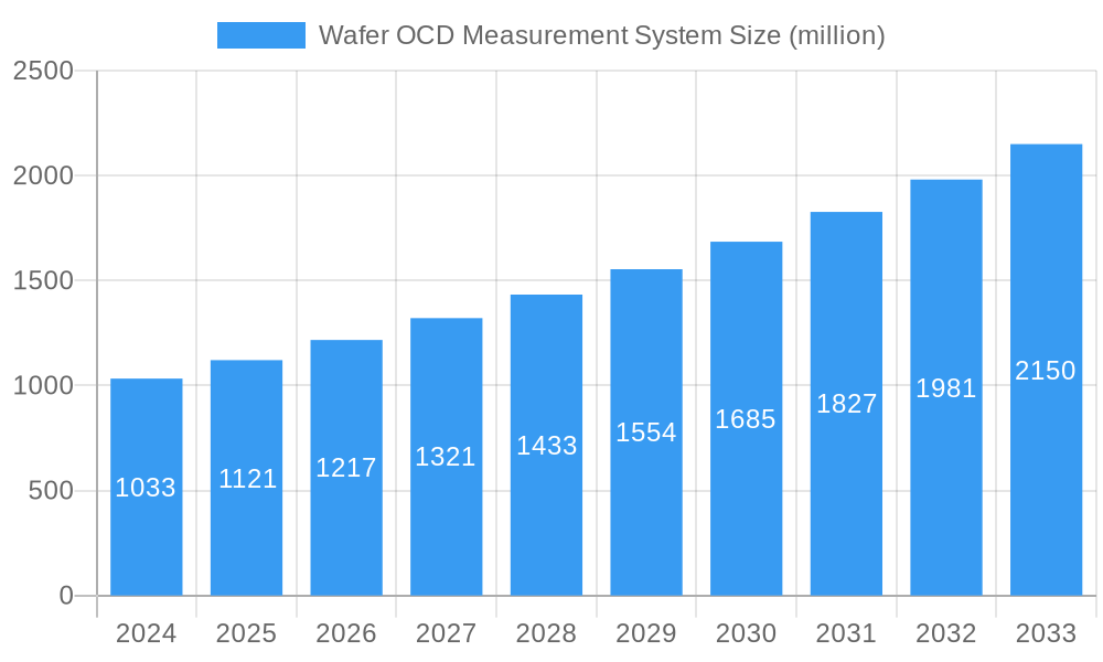
The Wafer Optical Critical Dimension (OCD) Measurement System market is poised for significant expansion, projected to reach an estimated $1033 million in 2024, driven by a robust CAGR of 8.6% through 2033. This growth is fundamentally fueled by the relentless pursuit of miniaturization and enhanced performance in semiconductor manufacturing. As leading chipmakers push towards increasingly advanced technical nodes, such as 7nm, 5nm, and below, the demand for precise and accurate metrology solutions like OCD systems escalates. These systems are indispensable for verifying critical dimensions and ensuring process control at sub-micron levels, thereby mitigating yield loss and guaranteeing the reliability of cutting-edge integrated circuits. The burgeoning adoption of 300mm wafers, which are the industry standard for high-volume production of advanced logic and memory chips, further amplifies the need for sophisticated OCD measurement capabilities. Innovations in sensor technology, advanced algorithms, and automation within OCD systems are also key drivers, enabling faster throughput and greater accuracy in a highly competitive foundry and integrated device manufacturer (IDM) landscape.
Wafer OCD Measurement System Market Size (In Billion)
The market's trajectory is also shaped by a dynamic interplay of trends and restraints. Emerging trends include the integration of AI and machine learning for predictive maintenance and real-time process correction in OCD systems, as well as the development of multi-modal metrology solutions that combine OCD with other techniques for comprehensive wafer inspection. The increasing complexity of 3D architectures in advanced chips necessitates more advanced OCD techniques capable of measuring intricate vertical structures. However, the market faces restraints such as the high initial investment cost of advanced OCD systems and the ongoing need for skilled personnel to operate and maintain them. Furthermore, the cyclical nature of the semiconductor industry, tied to global economic conditions and consumer demand for electronics, can introduce volatility. Despite these challenges, the indispensable role of OCD measurement systems in enabling the production of next-generation semiconductors, from high-performance computing to advanced mobile devices and automotive electronics, solidifies its strong growth prospects.
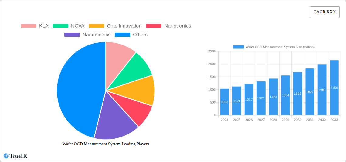
Wafer OCD Measurement System Company Market Share
Wafer OCD Measurement System Market: Comprehensive Analysis and Future Outlook (2019-2033)
This in-depth report provides a dynamic, SEO-optimized analysis of the global Wafer OCD Measurement System market. Leveraging high-volume keywords crucial for industry visibility, this study delves into market structure, competitive landscape, evolving trends, dominant segments, product innovations, key drivers, challenges, and the future outlook. With a study period spanning from 2019 to 2033, this comprehensive report offers invaluable insights for stakeholders navigating the complex semiconductor manufacturing ecosystem. The base year for estimations is 2025, with a detailed forecast period extending from 2025 to 2033, building upon historical data from 2019 to 2024.
Wafer OCD Measurement System Market Structure & Competitive Landscape
The Wafer OCD (Overlay Control and Defect) Measurement System market is characterized by a moderate to high level of concentration, with a few key players dominating significant market share. Innovation drivers are primarily centered around the relentless pursuit of shrinking transistor sizes and enhancing chip performance, necessitating highly precise and advanced metrology solutions. Regulatory impacts, while less direct than in other industries, pertain to industry standards for precision and data integrity in semiconductor manufacturing. Product substitutes, though limited in their direct replacement capabilities for OCD measurement, can emerge from advancements in alternative inspection techniques or integrated metrology solutions within the wafer fabrication process. End-user segmentation is heavily influenced by wafer size (200mm and 300mm) and the technological nodes being addressed, with a strong focus on advanced nodes like 7nm, 5nm, and below. Merger and acquisition (M&A) trends, while not always publicly disclosed in vast numbers, often reflect strategic consolidations aimed at acquiring complementary technologies or expanding market reach. For instance, historical M&A activity in the broader semiconductor equipment market suggests a pattern of consolidation to enhance R&D capabilities and offer comprehensive solutions. Anticipated M&A volumes are projected to be in the range of 10-20 million over the forecast period, driven by the need for integrated solutions and economies of scale. Concentration ratios for the top 3 players are estimated to be around 65-75% of the total market value, indicating a significant, albeit not fully monopolized, competitive environment.
Wafer OCD Measurement System Market Trends & Opportunities
The Wafer OCD Measurement System market is experiencing robust growth, driven by the escalating demand for advanced semiconductor devices across a multitude of industries. The market size is projected to witness a substantial expansion, with an estimated Compound Annual Growth Rate (CAGR) of approximately 12-15% over the forecast period (2025-2033). This impressive growth trajectory is underpinned by several key trends. Firstly, the relentless miniaturization of integrated circuits, pushing towards technical nodes of 5nm and even below, necessitates incredibly precise metrology tools capable of measuring features at the atomic level. Wafer OCD measurement systems are at the forefront of this advancement, ensuring critical overlay accuracy and critical dimension (CD) control, which are paramount for yield and performance. Secondly, the increasing complexity of semiconductor manufacturing processes, including multi-patterning and 3D stacking technologies, further amplifies the need for sophisticated OCD measurement solutions. These advanced techniques introduce new challenges in overlay and defect detection, creating a strong demand for cutting-edge metrology. Thirdly, the exponential growth in data consumption, fueled by AI, machine learning, 5G connectivity, and the Internet of Things (IoT), is driving the demand for higher-performance semiconductors, thereby indirectly stimulating the market for the equipment that produces them. Consumer preferences are increasingly aligned with devices offering greater processing power, lower energy consumption, and enhanced functionalities, all of which depend on advancements in semiconductor manufacturing. The competitive dynamics within the market are characterized by intense R&D investments and strategic partnerships aimed at developing next-generation OCD measurement technologies. Companies are focused on enhancing measurement speed, accuracy, and the ability to detect an ever-wider range of defects. Market penetration rates for advanced OCD measurement systems are steadily increasing, particularly in regions with high concentrations of leading-edge semiconductor fabrication plants. The ongoing transition of semiconductor manufacturing facilities to support the production of next-generation chips also presents significant opportunities for vendors of these critical metrology solutions. The average market penetration rate for state-of-the-art OCD measurement systems in leading-edge fabs is currently estimated to be around 70%, with strong potential for further growth as new fabs come online and existing ones are upgraded. The market opportunity is further augmented by the increasing adoption of automation and artificial intelligence in semiconductor manufacturing, where accurate and reliable metrology data is crucial for process control and optimization.
Dominant Markets & Segments in Wafer OCD Measurement System
The Wafer OCD Measurement System market exhibits distinct dominance across specific applications and technological nodes. Within the application segment, 300mm Wafer manufacturing stands out as the primary driver of market growth and revenue. The vast majority of advanced semiconductor production, particularly for cutting-edge logic and memory devices, utilizes 300mm wafers due to their higher throughput and cost-efficiency. This segment is projected to contribute over 75% of the total market revenue during the forecast period. While 200mm Wafer production remains significant, especially for mature technologies and specialized applications, its market share in terms of advanced OCD system demand is considerably lower, estimated at around 20%. The "Other" application segment, which may include emerging wafer technologies or research applications, represents a nascent but growing area with potential for future expansion.
In terms of technological nodes, the 5nm or Higher Technical Nodes segment is currently the most dominant and fastest-growing. This category encompasses the most advanced semiconductor manufacturing processes, requiring the highest levels of precision and sophisticated OCD measurement capabilities. The demand from this segment is projected to account for approximately 60% of the market revenue in 2025, with a significant upward trend. The 7nm segment follows closely, representing a substantial portion of the market with ongoing production and upgrade cycles, estimated to contribute around 25% of the revenue. The 1Xnm Technology Node and 2Xnm Technology Node segments, while still relevant, represent more mature technologies with a comparatively lower demand for the most advanced OCD systems. Their contribution is estimated to be around 10% and 5% respectively. However, the continued demand for cost-effective solutions in these segments ensures their continued market presence.
Key growth drivers for the dominance of 300mm wafers and advanced technical nodes include:
- Infrastructure Investment: Significant global investments in new leading-edge foundries and expansion of existing ones, primarily focused on 300mm wafer production for advanced logic and memory.
- Technological Advancements: The constant push for smaller, faster, and more power-efficient chips, which are only achievable with advanced lithography and stringent process control, necessitates cutting-edge OCD measurement.
- Demand from End Industries: The burgeoning demand for high-performance computing, AI accelerators, smartphones, and advanced automotive electronics directly fuels the need for semiconductors manufactured on 300mm wafers and at sub-7nm nodes.
- Government Policies & Subsidies: Many governments worldwide are actively promoting domestic semiconductor manufacturing through incentives and policies, often prioritizing the development of advanced node capabilities on 300mm wafers.
The market dominance is further reinforced by the concentration of intellectual property and manufacturing expertise within companies operating in these advanced segments. The high capital expenditure required for advanced fabrication plants naturally leads to a focus on state-of-the-art metrology, solidifying the leadership of 300mm wafers and the 5nm and below technical nodes in the Wafer OCD Measurement System market.
Wafer OCD Measurement System Product Analysis
Wafer OCD Measurement Systems are characterized by their continuous evolution towards higher precision, faster measurement speeds, and enhanced data analytics. Innovations focus on advanced optical techniques, sophisticated algorithms for data interpretation, and integrated automation for seamless workflow integration. These systems are critical for ensuring overlay accuracy, critical dimension control, and defect detection during complex lithography processes in semiconductor fabrication. Their competitive advantage lies in their ability to provide real-time, accurate, and actionable data, directly impacting wafer yield and manufacturing efficiency, especially for technical nodes of 7nm and below.
Key Drivers, Barriers & Challenges in Wafer OCD Measurement System
Key Drivers: The primary forces propelling the Wafer OCD Measurement System market include the insatiable demand for high-performance semiconductors driven by AI, 5G, and IoT. Technological advancements in lithography, such as EUV, necessitate increasingly precise metrology. Government initiatives supporting domestic chip manufacturing and R&D investments by leading semiconductor companies also act as significant growth catalysts. The economic imperative to improve wafer yield and reduce manufacturing costs further fuels the adoption of advanced OCD systems.
Key Challenges: Despite strong growth, the market faces challenges. The immense capital expenditure required for advanced OCD systems can be a barrier for smaller manufacturers. Supply chain disruptions, as witnessed in recent years, can impact the availability of critical components. Evolving regulatory landscapes regarding data security and manufacturing standards, though not a primary direct restraint, can influence operational requirements. Furthermore, intense competition among established players and emerging entrants, coupled with the long development cycles for new metrology technologies, poses competitive pressures. The estimated impact of supply chain issues on project timelines can range from 3-6 months, impacting new system deployments.
Growth Drivers in the Wafer OCD Measurement System Market
The growth drivers in the Wafer OCD Measurement System market are multifaceted, stemming from both technological advancements and market demand. The continuous push towards smaller and more powerful semiconductor devices, exemplified by the development of technical nodes of 7nm, 5nm, and below, fundamentally necessitates highly accurate overlay and critical dimension (CD) control, directly boosting the demand for advanced OCD systems. Furthermore, the burgeoning applications of Artificial Intelligence (AI), 5G networks, and the Internet of Things (IoT) are creating an unprecedented demand for sophisticated chips, thereby indirectly fueling the semiconductor manufacturing equipment market, including OCD measurement systems. Government initiatives and subsidies aimed at bolstering domestic semiconductor production capabilities in various regions also contribute significantly, encouraging investments in state-of-the-art manufacturing infrastructure.
Challenges Impacting Wafer OCD Measurement System Growth
Several barriers and restraints can impact the growth of the Wafer OCD Measurement System market. The extremely high cost of advanced OCD measurement equipment represents a significant capital investment, potentially limiting adoption by smaller or emerging semiconductor manufacturers. The intricate and globalized nature of the semiconductor supply chain also presents vulnerabilities, where disruptions in the availability of specialized components or raw materials can lead to delays in production and deployment of these sophisticated systems. Furthermore, the evolving landscape of international trade policies and geopolitical tensions can introduce uncertainties and affect market access in certain regions. Intense competition among established players, who constantly invest in R&D to maintain their technological edge, also creates pressure on pricing and market share.
Key Players Shaping the Wafer OCD Measurement System Market
- KLA
- NOVA
- Onto Innovation
- Nanotronics
- Nanometrics
- Shanghai RSIC
- Shanghai Precision Measurement
- Shenzhen Angstrom Excellence
- Shenzhen Chotest
- Suzhou TZTEK Technology
Significant Wafer OCD Measurement System Industry Milestones
- 2019: Introduction of advanced metrology algorithms for enhanced defect detection in multi-patterning processes.
- 2020: Significant investments in R&D by key players to develop OCD solutions for EUV lithography.
- 2021 (Q3): Launch of integrated metrology solutions combining OCD with other wafer inspection techniques.
- 2022 (H1): Strategic partnerships formed between OCD system manufacturers and leading semiconductor foundries to co-develop next-generation measurement capabilities.
- 2023 (Q4): Increased focus on AI-driven data analytics for predictive maintenance and process optimization in OCD systems.
- 2024 (H2): Development of enhanced software for faster data processing and improved user interface for OCD measurement platforms.
Future Outlook for Wafer OCD Measurement System Market
The future outlook for the Wafer OCD Measurement System market is exceptionally positive, driven by the sustained global demand for advanced semiconductors. The relentless pursuit of miniaturization in semiconductor technology, particularly towards 3nm and beyond, will continue to be the primary growth catalyst, necessitating increasingly sophisticated and accurate OCD measurement solutions. Emerging applications in areas like advanced packaging, flexible electronics, and specialized sensors will also contribute to market expansion. Strategic opportunities lie in the development of more integrated and intelligent metrology platforms that can offer real-time process feedback and adaptive control. The forecast period is expected to witness significant market potential as new foundries come online and existing ones upgrade their capabilities to meet the evolving demands of the digital economy. The market is projected to reach a substantial valuation, driven by innovation and the indispensable role of OCD measurement in modern semiconductor manufacturing.
Wafer OCD Measurement System Segmentation
-
1. Application
- 1.1. 200mm Wafer
- 1.2. 300mm Wafer
- 1.3. Other
-
2. Types
- 2.1. Technical Nodes Of 32nm and Below
- 2.2. 2Xnm Technology Node
- 2.3. 1Xnm Technology Node
- 2.4. 7nm, 5nm Or Higher Technical Nodes
Wafer OCD Measurement System Segmentation By Geography
-
1. North America
- 1.1. United States
- 1.2. Canada
- 1.3. Mexico
-
2. South America
- 2.1. Brazil
- 2.2. Argentina
- 2.3. Rest of South America
-
3. Europe
- 3.1. United Kingdom
- 3.2. Germany
- 3.3. France
- 3.4. Italy
- 3.5. Spain
- 3.6. Russia
- 3.7. Benelux
- 3.8. Nordics
- 3.9. Rest of Europe
-
4. Middle East & Africa
- 4.1. Turkey
- 4.2. Israel
- 4.3. GCC
- 4.4. North Africa
- 4.5. South Africa
- 4.6. Rest of Middle East & Africa
-
5. Asia Pacific
- 5.1. China
- 5.2. India
- 5.3. Japan
- 5.4. South Korea
- 5.5. ASEAN
- 5.6. Oceania
- 5.7. Rest of Asia Pacific
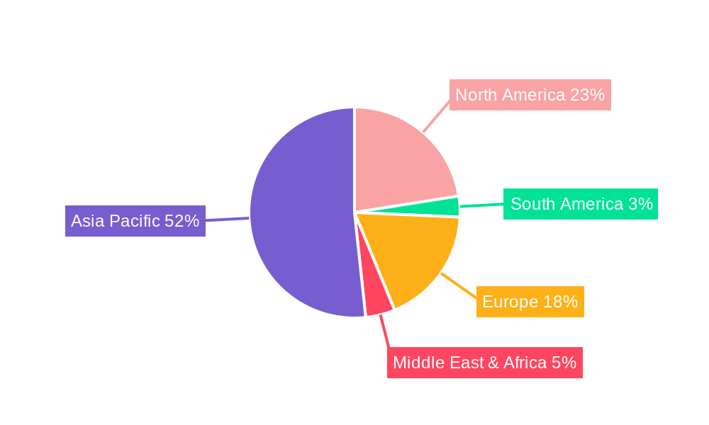
Wafer OCD Measurement System Regional Market Share
Geographic Coverage of Wafer OCD Measurement System
Wafer OCD Measurement System REPORT HIGHLIGHTS
| Aspects | Details |
|---|---|
| Study Period | 2020-2034 |
| Base Year | 2025 |
| Estimated Year | 2026 |
| Forecast Period | 2026-2034 |
| Historical Period | 2020-2025 |
| Growth Rate | CAGR of 8.6% from 2020-2034 |
| Segmentation |
|
Table of Contents
- 1. Introduction
- 1.1. Research Scope
- 1.2. Market Segmentation
- 1.3. Research Objective
- 1.4. Definitions and Assumptions
- 2. Executive Summary
- 2.1. Market Snapshot
- 3. Market Dynamics
- 3.1. Market Drivers
- 3.2. Market Restrains
- 3.3. Market Trends
- 3.4. Market Opportunities
- 4. Market Factor Analysis
- 4.1. Porters Five Forces
- 4.1.1. Bargaining Power of Suppliers
- 4.1.2. Bargaining Power of Buyers
- 4.1.3. Threat of New Entrants
- 4.1.4. Threat of Substitutes
- 4.1.5. Competitive Rivalry
- 4.2. PESTEL analysis
- 4.3. BCG Analysis
- 4.3.1. Stars (High Growth, High Market Share)
- 4.3.2. Cash Cows (Low Growth, High Market Share)
- 4.3.3. Question Mark (High Growth, Low Market Share)
- 4.3.4. Dogs (Low Growth, Low Market Share)
- 4.4. Ansoff Matrix Analysis
- 4.5. Supply Chain Analysis
- 4.6. Regulatory Landscape
- 4.7. Current Market Potential and Opportunity Assessment (TAM–SAM–SOM Framework)
- 4.8. TIR Analyst Note
- 4.1. Porters Five Forces
- 5. Market Analysis, Insights and Forecast 2021-2033
- 5.1. Market Analysis, Insights and Forecast - by Application
- 5.1.1. 200mm Wafer
- 5.1.2. 300mm Wafer
- 5.1.3. Other
- 5.2. Market Analysis, Insights and Forecast - by Types
- 5.2.1. Technical Nodes Of 32nm and Below
- 5.2.2. 2Xnm Technology Node
- 5.2.3. 1Xnm Technology Node
- 5.2.4. 7nm, 5nm Or Higher Technical Nodes
- 5.3. Market Analysis, Insights and Forecast - by Region
- 5.3.1. North America
- 5.3.2. South America
- 5.3.3. Europe
- 5.3.4. Middle East & Africa
- 5.3.5. Asia Pacific
- 5.1. Market Analysis, Insights and Forecast - by Application
- 6. Global Wafer OCD Measurement System Analysis, Insights and Forecast, 2021-2033
- 6.1. Market Analysis, Insights and Forecast - by Application
- 6.1.1. 200mm Wafer
- 6.1.2. 300mm Wafer
- 6.1.3. Other
- 6.2. Market Analysis, Insights and Forecast - by Types
- 6.2.1. Technical Nodes Of 32nm and Below
- 6.2.2. 2Xnm Technology Node
- 6.2.3. 1Xnm Technology Node
- 6.2.4. 7nm, 5nm Or Higher Technical Nodes
- 6.1. Market Analysis, Insights and Forecast - by Application
- 7. North America Wafer OCD Measurement System Analysis, Insights and Forecast, 2020-2032
- 7.1. Market Analysis, Insights and Forecast - by Application
- 7.1.1. 200mm Wafer
- 7.1.2. 300mm Wafer
- 7.1.3. Other
- 7.2. Market Analysis, Insights and Forecast - by Types
- 7.2.1. Technical Nodes Of 32nm and Below
- 7.2.2. 2Xnm Technology Node
- 7.2.3. 1Xnm Technology Node
- 7.2.4. 7nm, 5nm Or Higher Technical Nodes
- 7.1. Market Analysis, Insights and Forecast - by Application
- 8. South America Wafer OCD Measurement System Analysis, Insights and Forecast, 2020-2032
- 8.1. Market Analysis, Insights and Forecast - by Application
- 8.1.1. 200mm Wafer
- 8.1.2. 300mm Wafer
- 8.1.3. Other
- 8.2. Market Analysis, Insights and Forecast - by Types
- 8.2.1. Technical Nodes Of 32nm and Below
- 8.2.2. 2Xnm Technology Node
- 8.2.3. 1Xnm Technology Node
- 8.2.4. 7nm, 5nm Or Higher Technical Nodes
- 8.1. Market Analysis, Insights and Forecast - by Application
- 9. Europe Wafer OCD Measurement System Analysis, Insights and Forecast, 2020-2032
- 9.1. Market Analysis, Insights and Forecast - by Application
- 9.1.1. 200mm Wafer
- 9.1.2. 300mm Wafer
- 9.1.3. Other
- 9.2. Market Analysis, Insights and Forecast - by Types
- 9.2.1. Technical Nodes Of 32nm and Below
- 9.2.2. 2Xnm Technology Node
- 9.2.3. 1Xnm Technology Node
- 9.2.4. 7nm, 5nm Or Higher Technical Nodes
- 9.1. Market Analysis, Insights and Forecast - by Application
- 10. Middle East & Africa Wafer OCD Measurement System Analysis, Insights and Forecast, 2020-2032
- 10.1. Market Analysis, Insights and Forecast - by Application
- 10.1.1. 200mm Wafer
- 10.1.2. 300mm Wafer
- 10.1.3. Other
- 10.2. Market Analysis, Insights and Forecast - by Types
- 10.2.1. Technical Nodes Of 32nm and Below
- 10.2.2. 2Xnm Technology Node
- 10.2.3. 1Xnm Technology Node
- 10.2.4. 7nm, 5nm Or Higher Technical Nodes
- 10.1. Market Analysis, Insights and Forecast - by Application
- 11. Asia Pacific Wafer OCD Measurement System Analysis, Insights and Forecast, 2020-2032
- 11.1. Market Analysis, Insights and Forecast - by Application
- 11.1.1. 200mm Wafer
- 11.1.2. 300mm Wafer
- 11.1.3. Other
- 11.2. Market Analysis, Insights and Forecast - by Types
- 11.2.1. Technical Nodes Of 32nm and Below
- 11.2.2. 2Xnm Technology Node
- 11.2.3. 1Xnm Technology Node
- 11.2.4. 7nm, 5nm Or Higher Technical Nodes
- 11.1. Market Analysis, Insights and Forecast - by Application
- 12. Competitive Analysis
- 12.1. Company Profiles
- 12.1.1 KLA
- 12.1.1.1. Company Overview
- 12.1.1.2. Products
- 12.1.1.3. Company Financials
- 12.1.1.4. SWOT Analysis
- 12.1.2 NOVA
- 12.1.2.1. Company Overview
- 12.1.2.2. Products
- 12.1.2.3. Company Financials
- 12.1.2.4. SWOT Analysis
- 12.1.3 Onto Innovation
- 12.1.3.1. Company Overview
- 12.1.3.2. Products
- 12.1.3.3. Company Financials
- 12.1.3.4. SWOT Analysis
- 12.1.4 Nanotronics
- 12.1.4.1. Company Overview
- 12.1.4.2. Products
- 12.1.4.3. Company Financials
- 12.1.4.4. SWOT Analysis
- 12.1.5 Nanometrics
- 12.1.5.1. Company Overview
- 12.1.5.2. Products
- 12.1.5.3. Company Financials
- 12.1.5.4. SWOT Analysis
- 12.1.6 Shanghai RSIC
- 12.1.6.1. Company Overview
- 12.1.6.2. Products
- 12.1.6.3. Company Financials
- 12.1.6.4. SWOT Analysis
- 12.1.7 Shanghai Precision Measurement
- 12.1.7.1. Company Overview
- 12.1.7.2. Products
- 12.1.7.3. Company Financials
- 12.1.7.4. SWOT Analysis
- 12.1.8 Shenzhen Angstrom Excellence
- 12.1.8.1. Company Overview
- 12.1.8.2. Products
- 12.1.8.3. Company Financials
- 12.1.8.4. SWOT Analysis
- 12.1.9 Shenzhen Chotest
- 12.1.9.1. Company Overview
- 12.1.9.2. Products
- 12.1.9.3. Company Financials
- 12.1.9.4. SWOT Analysis
- 12.1.10 Suzhou TZTEK Technology
- 12.1.10.1. Company Overview
- 12.1.10.2. Products
- 12.1.10.3. Company Financials
- 12.1.10.4. SWOT Analysis
- 12.1.1 KLA
- 12.2. Market Entropy
- 12.2.1 Company's Key Areas Served
- 12.2.2 Recent Developments
- 12.3. Company Market Share Analysis 2025
- 12.3.1 Top 5 Companies Market Share Analysis
- 12.3.2 Top 3 Companies Market Share Analysis
- 12.4. List of Potential Customers
- 13. Research Methodology
List of Figures
- Figure 1: Global Wafer OCD Measurement System Revenue Breakdown (undefined, %) by Region 2025 & 2033
- Figure 2: North America Wafer OCD Measurement System Revenue (undefined), by Application 2025 & 2033
- Figure 3: North America Wafer OCD Measurement System Revenue Share (%), by Application 2025 & 2033
- Figure 4: North America Wafer OCD Measurement System Revenue (undefined), by Types 2025 & 2033
- Figure 5: North America Wafer OCD Measurement System Revenue Share (%), by Types 2025 & 2033
- Figure 6: North America Wafer OCD Measurement System Revenue (undefined), by Country 2025 & 2033
- Figure 7: North America Wafer OCD Measurement System Revenue Share (%), by Country 2025 & 2033
- Figure 8: South America Wafer OCD Measurement System Revenue (undefined), by Application 2025 & 2033
- Figure 9: South America Wafer OCD Measurement System Revenue Share (%), by Application 2025 & 2033
- Figure 10: South America Wafer OCD Measurement System Revenue (undefined), by Types 2025 & 2033
- Figure 11: South America Wafer OCD Measurement System Revenue Share (%), by Types 2025 & 2033
- Figure 12: South America Wafer OCD Measurement System Revenue (undefined), by Country 2025 & 2033
- Figure 13: South America Wafer OCD Measurement System Revenue Share (%), by Country 2025 & 2033
- Figure 14: Europe Wafer OCD Measurement System Revenue (undefined), by Application 2025 & 2033
- Figure 15: Europe Wafer OCD Measurement System Revenue Share (%), by Application 2025 & 2033
- Figure 16: Europe Wafer OCD Measurement System Revenue (undefined), by Types 2025 & 2033
- Figure 17: Europe Wafer OCD Measurement System Revenue Share (%), by Types 2025 & 2033
- Figure 18: Europe Wafer OCD Measurement System Revenue (undefined), by Country 2025 & 2033
- Figure 19: Europe Wafer OCD Measurement System Revenue Share (%), by Country 2025 & 2033
- Figure 20: Middle East & Africa Wafer OCD Measurement System Revenue (undefined), by Application 2025 & 2033
- Figure 21: Middle East & Africa Wafer OCD Measurement System Revenue Share (%), by Application 2025 & 2033
- Figure 22: Middle East & Africa Wafer OCD Measurement System Revenue (undefined), by Types 2025 & 2033
- Figure 23: Middle East & Africa Wafer OCD Measurement System Revenue Share (%), by Types 2025 & 2033
- Figure 24: Middle East & Africa Wafer OCD Measurement System Revenue (undefined), by Country 2025 & 2033
- Figure 25: Middle East & Africa Wafer OCD Measurement System Revenue Share (%), by Country 2025 & 2033
- Figure 26: Asia Pacific Wafer OCD Measurement System Revenue (undefined), by Application 2025 & 2033
- Figure 27: Asia Pacific Wafer OCD Measurement System Revenue Share (%), by Application 2025 & 2033
- Figure 28: Asia Pacific Wafer OCD Measurement System Revenue (undefined), by Types 2025 & 2033
- Figure 29: Asia Pacific Wafer OCD Measurement System Revenue Share (%), by Types 2025 & 2033
- Figure 30: Asia Pacific Wafer OCD Measurement System Revenue (undefined), by Country 2025 & 2033
- Figure 31: Asia Pacific Wafer OCD Measurement System Revenue Share (%), by Country 2025 & 2033
List of Tables
- Table 1: Global Wafer OCD Measurement System Revenue undefined Forecast, by Application 2020 & 2033
- Table 2: Global Wafer OCD Measurement System Revenue undefined Forecast, by Types 2020 & 2033
- Table 3: Global Wafer OCD Measurement System Revenue undefined Forecast, by Region 2020 & 2033
- Table 4: Global Wafer OCD Measurement System Revenue undefined Forecast, by Application 2020 & 2033
- Table 5: Global Wafer OCD Measurement System Revenue undefined Forecast, by Types 2020 & 2033
- Table 6: Global Wafer OCD Measurement System Revenue undefined Forecast, by Country 2020 & 2033
- Table 7: United States Wafer OCD Measurement System Revenue (undefined) Forecast, by Application 2020 & 2033
- Table 8: Canada Wafer OCD Measurement System Revenue (undefined) Forecast, by Application 2020 & 2033
- Table 9: Mexico Wafer OCD Measurement System Revenue (undefined) Forecast, by Application 2020 & 2033
- Table 10: Global Wafer OCD Measurement System Revenue undefined Forecast, by Application 2020 & 2033
- Table 11: Global Wafer OCD Measurement System Revenue undefined Forecast, by Types 2020 & 2033
- Table 12: Global Wafer OCD Measurement System Revenue undefined Forecast, by Country 2020 & 2033
- Table 13: Brazil Wafer OCD Measurement System Revenue (undefined) Forecast, by Application 2020 & 2033
- Table 14: Argentina Wafer OCD Measurement System Revenue (undefined) Forecast, by Application 2020 & 2033
- Table 15: Rest of South America Wafer OCD Measurement System Revenue (undefined) Forecast, by Application 2020 & 2033
- Table 16: Global Wafer OCD Measurement System Revenue undefined Forecast, by Application 2020 & 2033
- Table 17: Global Wafer OCD Measurement System Revenue undefined Forecast, by Types 2020 & 2033
- Table 18: Global Wafer OCD Measurement System Revenue undefined Forecast, by Country 2020 & 2033
- Table 19: United Kingdom Wafer OCD Measurement System Revenue (undefined) Forecast, by Application 2020 & 2033
- Table 20: Germany Wafer OCD Measurement System Revenue (undefined) Forecast, by Application 2020 & 2033
- Table 21: France Wafer OCD Measurement System Revenue (undefined) Forecast, by Application 2020 & 2033
- Table 22: Italy Wafer OCD Measurement System Revenue (undefined) Forecast, by Application 2020 & 2033
- Table 23: Spain Wafer OCD Measurement System Revenue (undefined) Forecast, by Application 2020 & 2033
- Table 24: Russia Wafer OCD Measurement System Revenue (undefined) Forecast, by Application 2020 & 2033
- Table 25: Benelux Wafer OCD Measurement System Revenue (undefined) Forecast, by Application 2020 & 2033
- Table 26: Nordics Wafer OCD Measurement System Revenue (undefined) Forecast, by Application 2020 & 2033
- Table 27: Rest of Europe Wafer OCD Measurement System Revenue (undefined) Forecast, by Application 2020 & 2033
- Table 28: Global Wafer OCD Measurement System Revenue undefined Forecast, by Application 2020 & 2033
- Table 29: Global Wafer OCD Measurement System Revenue undefined Forecast, by Types 2020 & 2033
- Table 30: Global Wafer OCD Measurement System Revenue undefined Forecast, by Country 2020 & 2033
- Table 31: Turkey Wafer OCD Measurement System Revenue (undefined) Forecast, by Application 2020 & 2033
- Table 32: Israel Wafer OCD Measurement System Revenue (undefined) Forecast, by Application 2020 & 2033
- Table 33: GCC Wafer OCD Measurement System Revenue (undefined) Forecast, by Application 2020 & 2033
- Table 34: North Africa Wafer OCD Measurement System Revenue (undefined) Forecast, by Application 2020 & 2033
- Table 35: South Africa Wafer OCD Measurement System Revenue (undefined) Forecast, by Application 2020 & 2033
- Table 36: Rest of Middle East & Africa Wafer OCD Measurement System Revenue (undefined) Forecast, by Application 2020 & 2033
- Table 37: Global Wafer OCD Measurement System Revenue undefined Forecast, by Application 2020 & 2033
- Table 38: Global Wafer OCD Measurement System Revenue undefined Forecast, by Types 2020 & 2033
- Table 39: Global Wafer OCD Measurement System Revenue undefined Forecast, by Country 2020 & 2033
- Table 40: China Wafer OCD Measurement System Revenue (undefined) Forecast, by Application 2020 & 2033
- Table 41: India Wafer OCD Measurement System Revenue (undefined) Forecast, by Application 2020 & 2033
- Table 42: Japan Wafer OCD Measurement System Revenue (undefined) Forecast, by Application 2020 & 2033
- Table 43: South Korea Wafer OCD Measurement System Revenue (undefined) Forecast, by Application 2020 & 2033
- Table 44: ASEAN Wafer OCD Measurement System Revenue (undefined) Forecast, by Application 2020 & 2033
- Table 45: Oceania Wafer OCD Measurement System Revenue (undefined) Forecast, by Application 2020 & 2033
- Table 46: Rest of Asia Pacific Wafer OCD Measurement System Revenue (undefined) Forecast, by Application 2020 & 2033
Frequently Asked Questions
1. What is the projected Compound Annual Growth Rate (CAGR) of the Wafer OCD Measurement System?
The projected CAGR is approximately 8.6%.
2. Which companies are prominent players in the Wafer OCD Measurement System?
Key companies in the market include KLA, NOVA, Onto Innovation, Nanotronics, Nanometrics, Shanghai RSIC, Shanghai Precision Measurement, Shenzhen Angstrom Excellence, Shenzhen Chotest, Suzhou TZTEK Technology.
3. What are the main segments of the Wafer OCD Measurement System?
The market segments include Application, Types.
4. Can you provide details about the market size?
The market size is estimated to be USD XXX N/A as of 2022.
5. What are some drivers contributing to market growth?
N/A
6. What are the notable trends driving market growth?
N/A
7. Are there any restraints impacting market growth?
N/A
8. Can you provide examples of recent developments in the market?
N/A
9. What pricing options are available for accessing the report?
Pricing options include single-user, multi-user, and enterprise licenses priced at USD 2900.00, USD 4350.00, and USD 5800.00 respectively.
10. Is the market size provided in terms of value or volume?
The market size is provided in terms of value, measured in N/A.
11. Are there any specific market keywords associated with the report?
Yes, the market keyword associated with the report is "Wafer OCD Measurement System," which aids in identifying and referencing the specific market segment covered.
12. How do I determine which pricing option suits my needs best?
The pricing options vary based on user requirements and access needs. Individual users may opt for single-user licenses, while businesses requiring broader access may choose multi-user or enterprise licenses for cost-effective access to the report.
13. Are there any additional resources or data provided in the Wafer OCD Measurement System report?
While the report offers comprehensive insights, it's advisable to review the specific contents or supplementary materials provided to ascertain if additional resources or data are available.
14. How can I stay updated on further developments or reports in the Wafer OCD Measurement System?
To stay informed about further developments, trends, and reports in the Wafer OCD Measurement System, consider subscribing to industry newsletters, following relevant companies and organizations, or regularly checking reputable industry news sources and publications.
Methodology
Step 1 - Identification of Relevant Samples Size from Population Database


Step 2 - Approaches for Defining Global Market Size (Value, Volume* & Price*)

Note*: In applicable scenarios
Step 3 - Data Sources
Primary Research
- Web Analytics
- Survey Reports
- Research Institute
- Latest Research Reports
- Opinion Leaders
Secondary Research
- Annual Reports
- White Paper
- Latest Press Release
- Industry Association
- Paid Database
- Investor Presentations

Step 4 - Data Triangulation
Involves using different sources of information in order to increase the validity of a study
These sources are likely to be stakeholders in a program - participants, other researchers, program staff, other community members, and so on.
Then we put all data in single framework & apply various statistical tools to find out the dynamic on the market.
During the analysis stage, feedback from the stakeholder groups would be compared to determine areas of agreement as well as areas of divergence