

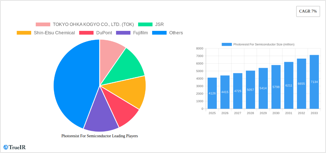
Key Insights
The global Photoresist for Semiconductor market is poised for significant expansion, projected to reach an estimated $4126 million by 2025, driven by a compound annual growth rate (CAGR) of 7%. This robust growth is underpinned by the relentless demand for advanced semiconductor devices across a myriad of consumer electronics, automotive, and industrial applications. Key market drivers include the escalating adoption of smartphones, wearables, and the burgeoning Internet of Things (IoT) ecosystem, all of which necessitate increasingly sophisticated and miniaturized semiconductor components. Furthermore, the rapid evolution of Artificial Intelligence (AI), 5G infrastructure deployment, and the increasing complexity of data centers are fueling the need for high-performance chips, thereby boosting the consumption of specialized photoresists. The continuous innovation in semiconductor manufacturing processes, particularly the transition to advanced lithography techniques such as Extreme Ultraviolet (EUV) lithography and multi-patterning, also acts as a significant growth catalyst.
Photoresist For Semiconductor Market Size (In Billion)
The market is segmented into distinct categories based on application, including Positive Photoresists and Negative Photoresists, and by type, encompassing EUV Photoresists, ArF Photoresists, KrF Photoresists, g/i-Line Photoresists, and Electronic Beam (EB) Photoresists. The growing prominence of EUV photoresists, essential for fabricating sub-10nm semiconductor nodes, is a notable trend. However, certain factors present challenges to market expansion. The high cost associated with advanced lithography equipment, particularly for EUV, and the stringent purity requirements for photoresist materials can pose significant barriers to entry and operational expenses for manufacturers. Moreover, the complex and cyclical nature of the semiconductor industry, influenced by global economic conditions and supply chain volatilities, can also impact market dynamics. Despite these restraints, the overarching trend towards miniaturization, enhanced performance, and increased functionality in electronic devices ensures a consistently strong demand for advanced photoresist solutions.

Photoresist For Semiconductor Company Market Share
Advanced Photoresist Solutions for Next-Generation Semiconductors: A Comprehensive Market Report (2019-2033)
This in-depth report provides an authoritative analysis of the global photoresist for semiconductor market, examining its structure, trends, opportunities, and competitive landscape. Spanning from 2019 to 2033, with a base and estimated year of 2025, this report offers critical insights for stakeholders navigating the dynamic semiconductor manufacturing ecosystem. The analysis leverages high-volume keywords such as "semiconductor photoresists," "EUV photoresists," "ArF photoresists," "lithography chemicals," "microelectronics," and "advanced packaging" to enhance SEO visibility and reach a targeted industry audience.
Photoresist For Semiconductor Market Structure & Competitive Landscape
The global photoresist for semiconductor market is characterized by a moderate to high concentration, driven by the significant capital investment required for research, development, and high-volume manufacturing. Innovation remains a paramount driver, with continuous efforts focused on achieving higher resolution, improved sensitivity, and enhanced performance for advanced lithography techniques like Extreme Ultraviolet (EUV) and ArF immersion. Regulatory impacts, primarily concerning environmental standards and chemical safety, also shape market strategies and product development. While direct product substitutes are limited due to the specialized nature of photoresists, advancements in alternative lithography technologies (though currently nascent for high-volume semiconductor manufacturing) represent a potential long-term disruptive force. End-user segmentation primarily revolves around leading semiconductor foundries and Integrated Device Manufacturers (IDMs) that utilize these critical materials in their fabrication processes. Merger and acquisition (M&A) activities, while not as frequent as in broader chemical markets, occur periodically to consolidate technological capabilities, expand geographic reach, and secure intellectual property. The top 5 players are estimated to hold approximately 70% of the market share, with a notable increase in M&A activity in the historical period (2019-2024) focused on acquiring specialized lithography additive companies and innovative EUV photoresist formulations, accounting for an estimated 5 M&A deals valued at over $200 million annually.
Photoresist For Semiconductor Market Trends & Opportunities
The global photoresist for semiconductor market is experiencing robust growth, projected to reach a market size exceeding $3 billion by 2025. This expansion is fueled by the relentless demand for more powerful and energy-efficient electronic devices, driving the need for advanced semiconductor nodes and sophisticated lithography solutions. The market size has demonstrated a consistent Compound Annual Growth Rate (CAGR) of approximately 8% over the historical period (2019-2024) and is expected to maintain a CAGR of around 7.5% during the forecast period (2025-2033). Technological shifts are profoundly influencing market dynamics, with a significant surge in the adoption of EUV photoresists as leading foundries push the boundaries of transistor scaling, enabling the production of 3nm and below semiconductor nodes. This transition from traditional KrF and ArF lithography to EUV represents a major paradigm shift, requiring substantial R&D investment and a deep understanding of photochemistry. Consumer preferences for smaller, faster, and more integrated electronic devices, ranging from smartphones and AI accelerators to automotive electronics and IoT devices, are directly translating into increased demand for high-performance photoresists. Competitive dynamics are intensifying, with established players continuously innovating to meet the stringent requirements of advanced lithography, while new entrants are exploring niche applications and novel material formulations. Market penetration rates for advanced photoresists, particularly EUV and ArF immersion, are steadily increasing, driven by the transition to next-generation fabrication processes. Opportunities abound for suppliers who can offer customized solutions, superior technical support, and consistent product quality, especially in emerging markets with growing semiconductor manufacturing capabilities. The demand for specialized photoresists for advanced packaging techniques, such as chiplets and 3D integration, is also a significant growth vector, creating new avenues for innovation and market expansion. The pursuit of higher yields and reduced defect rates in semiconductor manufacturing also pushes the demand for photoresists with enhanced process latitude and reduced variability.
Dominant Markets & Segments in Photoresist For Semiconductor
The Asia-Pacific region stands out as the dominant market for photoresists in the semiconductor industry, driven by its expansive semiconductor manufacturing base. Countries such as South Korea, Taiwan, and Japan are at the forefront of advanced semiconductor fabrication, hosting the world's leading foundries and IDMs. This dominance is underpinned by significant government initiatives promoting domestic semiconductor production, substantial investments in research and development, and the presence of a highly skilled workforce.
Within the Application segment, Positive Photoresists continue to hold a significant market share, accounting for over 75% of the total demand. This is primarily due to their widespread use in established and advanced lithography processes requiring high resolution and precise pattern transfer.
The Type segment is witnessing a substantial shift towards advanced lithography chemistries:
- EUV Photoresists: While currently a smaller segment in terms of volume, EUV photoresists represent the most rapidly growing and strategically important category. The commercialization of EUV lithography for high-volume manufacturing of leading-edge chips (e.g., 7nm, 5nm, and beyond) is a primary growth driver. The demand for EUV photoresists is projected to grow at a CAGR of over 20% from 2025-2033, driven by increasing adoption by major foundries for their most advanced process nodes.
- ArF Photoresists: ArF immersion photoresists remain critical for advanced nodes (e.g., 10nm to 7nm) where EUV is not yet fully deployed or is used in conjunction with multi-patterning. The market for ArF photoresists is stable, with ongoing innovation focused on improving performance for sub-10nm nodes.
- KrF Photoresists: These continue to be vital for manufacturing mature and legacy semiconductor nodes, representing a substantial portion of the market volume. Their demand is expected to remain steady, driven by the vast installed base of fabrication equipment for these technologies.
- g/i-Line Photoresists: Primarily used in less critical lithography applications and for manufacturing less advanced semiconductor devices, g/i-line photoresists continue to serve a significant market segment.
- Electronic Beam (EB) Photoresists: While not used in high-volume semiconductor manufacturing, EB photoresists are crucial for mask making and R&D. Their demand is driven by the need for high-resolution patterning in photomask production.
Key growth drivers in dominant segments include:
- Infrastructure Development: Massive investments in new semiconductor fabrication plants (fabs) in Asia, particularly in South Korea and Taiwan, are directly translating into increased demand for all types of photoresists.
- Policies: Government incentives and strategic national semiconductor initiatives in key Asian economies are accelerating market growth and attracting new investments.
- Technological Advancements: The continuous push for Moore's Law and advanced semiconductor architectures necessitates the development and adoption of cutting-edge photoresist materials capable of finer feature sizes and higher densities.
Photoresist For Semiconductor Product Analysis
Product innovations in the photoresist for semiconductor market are primarily centered on enhancing resolution, sensitivity, and process latitude for increasingly sophisticated lithography techniques. The development of novel EUV photoresists with advanced chemistries that minimize outgassing and maximize line edge roughness (LER) is a critical area of focus. ArF immersion photoresists are being refined to achieve better performance at sub-10nm nodes, often incorporating new resist architectures and advanced developers. For mature nodes, improvements in cost-effectiveness and environmental sustainability are key. Competitive advantages are gained through proprietary formulations, superior material purity, consistent batch-to-batch quality, and strong technical support for process integration. Companies are also innovating in photoresist ancillary materials, such as developers, removers, and anti-reflective coatings (ARCs), to optimize the entire lithography process.
Key Drivers, Barriers & Challenges in Photoresist For Semiconductor
Key Drivers: The semiconductor industry's insatiable demand for smaller, faster, and more powerful chips is the primary driver. This is fueled by advancements in artificial intelligence, 5G, IoT, and high-performance computing. The ongoing transition to advanced lithography technologies like EUV necessitates continuous innovation and high-performance photoresists. Government support and investments in semiconductor manufacturing capacity globally, particularly in Asia, further propel market growth.
Key Barriers & Challenges: High R&D costs and the lengthy development cycles for new photoresist formulations represent significant barriers to entry. The extremely stringent purity and quality control requirements for semiconductor-grade chemicals add to manufacturing complexity and cost. Supply chain disruptions, especially for rare earth elements or specialized precursors, can impact production. Intense competition among established players and the threat of alternative lithography technologies, though a long-term concern, also present challenges. Furthermore, increasing environmental regulations and the need for sustainable manufacturing practices require ongoing adaptation.
Growth Drivers in the Photoresist For Semiconductor Market
The growth of the photoresist for semiconductor market is predominantly propelled by the relentless pursuit of technological advancements in the semiconductor industry. The ever-increasing demand for higher processing power and miniaturization in consumer electronics, automotive, and data centers necessitates the continuous shrinking of transistor feature sizes. This directly translates into a higher demand for advanced photoresist materials, especially for cutting-edge lithography techniques such as EUV and ArF immersion. Strategic governmental initiatives worldwide, aimed at bolstering domestic semiconductor manufacturing capabilities and ensuring supply chain resilience, are also providing significant impetus. For instance, significant financial incentives and policy support in regions like North America and Europe are encouraging the establishment of new fabs, which in turn will drive the demand for photoresist materials. The expanding application of semiconductors in emerging sectors like electric vehicles, AI, and the Internet of Things (IoT) further solidifies the long-term growth trajectory of the photoresist market.
Challenges Impacting Photoresist For Semiconductor Growth
The photoresist for semiconductor market faces several significant challenges that can impact its growth trajectory. The stringent purity and consistency requirements for semiconductor-grade materials necessitate highly complex and expensive manufacturing processes, leading to high production costs and significant barriers to entry for new players. The lengthy development and qualification cycles for new photoresist formulations, often spanning several years, can hinder the rapid adoption of innovative solutions. Furthermore, the global supply chain for raw materials used in photoresist manufacturing can be vulnerable to disruptions caused by geopolitical events, natural disasters, or trade restrictions, potentially leading to shortages and price volatility. The evolving regulatory landscape concerning environmental impact and chemical safety adds another layer of complexity, requiring continuous adaptation and investment in compliance. Intense competition among established players and the ongoing drive for cost reduction by semiconductor manufacturers also exert considerable pressure on profit margins.
Key Players Shaping the Photoresist For Semiconductor Market
- TOKYO OHKA KOGYO CO., LTD. (TOK)
- JSR
- Shin-Etsu Chemical
- DuPont
- Fujifilm
- Sumitomo Chemical
- Dongjin Semichem
- Merck KGaA (AZ)
- Allresist GmbH
- Futurrex
- KemLab™ Inc
- YCCHEM Co., Ltd
- SK Materials Performance (SKMP)
- Everlight Chemical
- Red Avenue
- Crystal Clear Electronic Material
- Xuzhou B & C Chemical
- Xiamen Hengkun New Material Technology
- Jiangsu Aisen Semiconductor Material
- Zhuhai Cornerstone Technologies
- Shanghai Sinyang Semiconductor Materials
- ShenZhen RongDa Photosensitive Science & Technology
- SINEVA
- Guoke Tianji
- Jiangsu Nata Opto-electronic Material
- PhiChem
Significant Photoresist For Semiconductor Industry Milestones
- 2019: Introduction of commercially viable EUV photoresists by leading suppliers, marking a pivotal moment for next-generation semiconductor manufacturing.
- 2020: Major semiconductor foundries begin high-volume production using EUV lithography, accelerating demand for EUV photoresists.
- 2021: Increased investment in R&D for next-generation ArF immersion photoresists to support sub-7nm nodes.
- 2022: Growing emphasis on developing more sustainable and environmentally friendly photoresist formulations.
- 2023: Significant expansion of semiconductor manufacturing capacity in Asia, driving demand for various photoresist types.
- 2024: Advancements in photoresist ancillary materials (developers, strippers) to optimize lithography process windows and yield.
- 2025 (Estimated): Further commercialization of EUV lithography for even more advanced process nodes, leading to increased market share for EUV photoresists.
- 2026-2033 (Forecast): Continued innovation in EUV and exploration of future lithography technologies like High-NA EUV, driving demand for novel photoresist chemistries and materials.
Future Outlook for Photoresist For Semiconductor Market
The future outlook for the photoresist for semiconductor market is exceptionally bright, driven by the sustained demand for advanced semiconductor technologies. The continued expansion of EUV lithography for critical layers in leading-edge chip manufacturing will remain a primary growth catalyst, necessitating ongoing advancements in EUV photoresist performance and reliability. Opportunities are also emerging in the development of specialized photoresists for advanced packaging techniques, such as 3D stacking and heterogeneous integration, to enable continued device performance improvements. Strategic investments in new semiconductor fabrication facilities globally, coupled with government support for domestic production, will further bolster market demand. The increasing integration of AI, 5G, and automotive electronics into everyday life will continue to fuel the need for more sophisticated and efficient semiconductor devices, thereby creating a robust and expanding market for high-performance photoresists. Players who can innovate, ensure supply chain stability, and meet stringent quality demands will be well-positioned for significant growth in the coming years.
Photoresist For Semiconductor Segmentation
-
1. Application
- 1.1. Positive Photoresists
- 1.2. Negative Photoresists
-
2. Type
- 2.1. EUV Photoresists
- 2.2. ArF Photoresists
- 2.3. KrF Photoresists
- 2.4. g/i-Line Photoresists
- 2.5. Electronic Beam (EB) Photoresists
Photoresist For Semiconductor Segmentation By Geography
-
1. North America
- 1.1. United States
- 1.2. Canada
- 1.3. Mexico
-
2. South America
- 2.1. Brazil
- 2.2. Argentina
- 2.3. Rest of South America
-
3. Europe
- 3.1. United Kingdom
- 3.2. Germany
- 3.3. France
- 3.4. Italy
- 3.5. Spain
- 3.6. Russia
- 3.7. Benelux
- 3.8. Nordics
- 3.9. Rest of Europe
-
4. Middle East & Africa
- 4.1. Turkey
- 4.2. Israel
- 4.3. GCC
- 4.4. North Africa
- 4.5. South Africa
- 4.6. Rest of Middle East & Africa
-
5. Asia Pacific
- 5.1. China
- 5.2. India
- 5.3. Japan
- 5.4. South Korea
- 5.5. ASEAN
- 5.6. Oceania
- 5.7. Rest of Asia Pacific
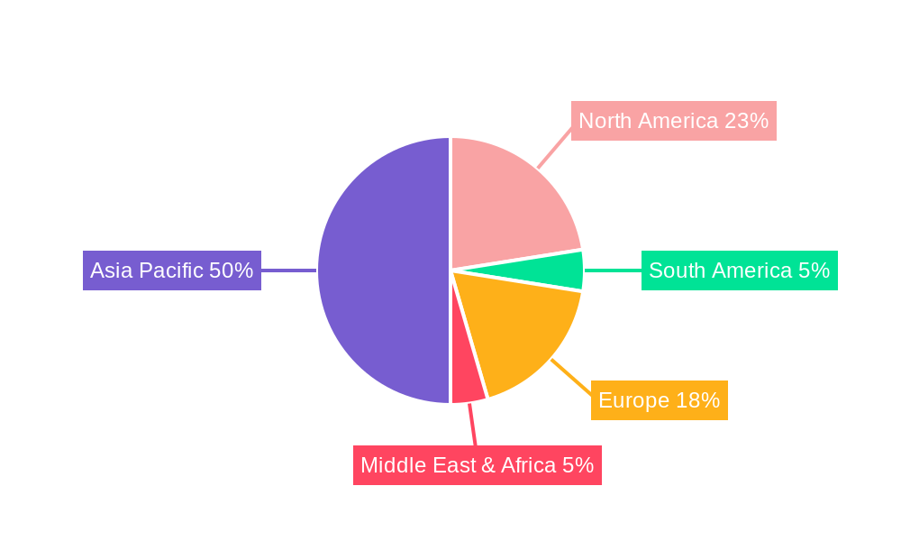
Photoresist For Semiconductor Regional Market Share
Geographic Coverage of Photoresist For Semiconductor
Photoresist For Semiconductor REPORT HIGHLIGHTS
| Aspects | Details |
|---|---|
| Study Period | 2020-2034 |
| Base Year | 2025 |
| Estimated Year | 2026 |
| Forecast Period | 2026-2034 |
| Historical Period | 2020-2025 |
| Growth Rate | CAGR of 7% from 2020-2034 |
| Segmentation |
|
Table of Contents
- 1. Introduction
- 1.1. Research Scope
- 1.2. Market Segmentation
- 1.3. Research Methodology
- 1.4. Definitions and Assumptions
- 2. Executive Summary
- 2.1. Introduction
- 3. Market Dynamics
- 3.1. Introduction
- 3.2. Market Drivers
- 3.3. Market Restrains
- 3.4. Market Trends
- 4. Market Factor Analysis
- 4.1. Porters Five Forces
- 4.2. Supply/Value Chain
- 4.3. PESTEL analysis
- 4.4. Market Entropy
- 4.5. Patent/Trademark Analysis
- 5. Global Photoresist For Semiconductor Analysis, Insights and Forecast, 2020-2032
- 5.1. Market Analysis, Insights and Forecast - by Application
- 5.1.1. Positive Photoresists
- 5.1.2. Negative Photoresists
- 5.2. Market Analysis, Insights and Forecast - by Type
- 5.2.1. EUV Photoresists
- 5.2.2. ArF Photoresists
- 5.2.3. KrF Photoresists
- 5.2.4. g/i-Line Photoresists
- 5.2.5. Electronic Beam (EB) Photoresists
- 5.3. Market Analysis, Insights and Forecast - by Region
- 5.3.1. North America
- 5.3.2. South America
- 5.3.3. Europe
- 5.3.4. Middle East & Africa
- 5.3.5. Asia Pacific
- 5.1. Market Analysis, Insights and Forecast - by Application
- 6. North America Photoresist For Semiconductor Analysis, Insights and Forecast, 2020-2032
- 6.1. Market Analysis, Insights and Forecast - by Application
- 6.1.1. Positive Photoresists
- 6.1.2. Negative Photoresists
- 6.2. Market Analysis, Insights and Forecast - by Type
- 6.2.1. EUV Photoresists
- 6.2.2. ArF Photoresists
- 6.2.3. KrF Photoresists
- 6.2.4. g/i-Line Photoresists
- 6.2.5. Electronic Beam (EB) Photoresists
- 6.1. Market Analysis, Insights and Forecast - by Application
- 7. South America Photoresist For Semiconductor Analysis, Insights and Forecast, 2020-2032
- 7.1. Market Analysis, Insights and Forecast - by Application
- 7.1.1. Positive Photoresists
- 7.1.2. Negative Photoresists
- 7.2. Market Analysis, Insights and Forecast - by Type
- 7.2.1. EUV Photoresists
- 7.2.2. ArF Photoresists
- 7.2.3. KrF Photoresists
- 7.2.4. g/i-Line Photoresists
- 7.2.5. Electronic Beam (EB) Photoresists
- 7.1. Market Analysis, Insights and Forecast - by Application
- 8. Europe Photoresist For Semiconductor Analysis, Insights and Forecast, 2020-2032
- 8.1. Market Analysis, Insights and Forecast - by Application
- 8.1.1. Positive Photoresists
- 8.1.2. Negative Photoresists
- 8.2. Market Analysis, Insights and Forecast - by Type
- 8.2.1. EUV Photoresists
- 8.2.2. ArF Photoresists
- 8.2.3. KrF Photoresists
- 8.2.4. g/i-Line Photoresists
- 8.2.5. Electronic Beam (EB) Photoresists
- 8.1. Market Analysis, Insights and Forecast - by Application
- 9. Middle East & Africa Photoresist For Semiconductor Analysis, Insights and Forecast, 2020-2032
- 9.1. Market Analysis, Insights and Forecast - by Application
- 9.1.1. Positive Photoresists
- 9.1.2. Negative Photoresists
- 9.2. Market Analysis, Insights and Forecast - by Type
- 9.2.1. EUV Photoresists
- 9.2.2. ArF Photoresists
- 9.2.3. KrF Photoresists
- 9.2.4. g/i-Line Photoresists
- 9.2.5. Electronic Beam (EB) Photoresists
- 9.1. Market Analysis, Insights and Forecast - by Application
- 10. Asia Pacific Photoresist For Semiconductor Analysis, Insights and Forecast, 2020-2032
- 10.1. Market Analysis, Insights and Forecast - by Application
- 10.1.1. Positive Photoresists
- 10.1.2. Negative Photoresists
- 10.2. Market Analysis, Insights and Forecast - by Type
- 10.2.1. EUV Photoresists
- 10.2.2. ArF Photoresists
- 10.2.3. KrF Photoresists
- 10.2.4. g/i-Line Photoresists
- 10.2.5. Electronic Beam (EB) Photoresists
- 10.1. Market Analysis, Insights and Forecast - by Application
- 11. Competitive Analysis
- 11.1. Global Market Share Analysis 2025
- 11.2. Company Profiles
- 11.2.1 TOKYO OHKA KOGYO CO. LTD. (TOK)
- 11.2.1.1. Overview
- 11.2.1.2. Products
- 11.2.1.3. SWOT Analysis
- 11.2.1.4. Recent Developments
- 11.2.1.5. Financials (Based on Availability)
- 11.2.2 JSR
- 11.2.2.1. Overview
- 11.2.2.2. Products
- 11.2.2.3. SWOT Analysis
- 11.2.2.4. Recent Developments
- 11.2.2.5. Financials (Based on Availability)
- 11.2.3 Shin-Etsu Chemical
- 11.2.3.1. Overview
- 11.2.3.2. Products
- 11.2.3.3. SWOT Analysis
- 11.2.3.4. Recent Developments
- 11.2.3.5. Financials (Based on Availability)
- 11.2.4 DuPont
- 11.2.4.1. Overview
- 11.2.4.2. Products
- 11.2.4.3. SWOT Analysis
- 11.2.4.4. Recent Developments
- 11.2.4.5. Financials (Based on Availability)
- 11.2.5 Fujifilm
- 11.2.5.1. Overview
- 11.2.5.2. Products
- 11.2.5.3. SWOT Analysis
- 11.2.5.4. Recent Developments
- 11.2.5.5. Financials (Based on Availability)
- 11.2.6 Sumitomo Chemical
- 11.2.6.1. Overview
- 11.2.6.2. Products
- 11.2.6.3. SWOT Analysis
- 11.2.6.4. Recent Developments
- 11.2.6.5. Financials (Based on Availability)
- 11.2.7 Dongjin Semichem
- 11.2.7.1. Overview
- 11.2.7.2. Products
- 11.2.7.3. SWOT Analysis
- 11.2.7.4. Recent Developments
- 11.2.7.5. Financials (Based on Availability)
- 11.2.8 Merck KGaA (AZ)
- 11.2.8.1. Overview
- 11.2.8.2. Products
- 11.2.8.3. SWOT Analysis
- 11.2.8.4. Recent Developments
- 11.2.8.5. Financials (Based on Availability)
- 11.2.9 Allresist GmbH
- 11.2.9.1. Overview
- 11.2.9.2. Products
- 11.2.9.3. SWOT Analysis
- 11.2.9.4. Recent Developments
- 11.2.9.5. Financials (Based on Availability)
- 11.2.10 Futurrex
- 11.2.10.1. Overview
- 11.2.10.2. Products
- 11.2.10.3. SWOT Analysis
- 11.2.10.4. Recent Developments
- 11.2.10.5. Financials (Based on Availability)
- 11.2.11 KemLab™ Inc
- 11.2.11.1. Overview
- 11.2.11.2. Products
- 11.2.11.3. SWOT Analysis
- 11.2.11.4. Recent Developments
- 11.2.11.5. Financials (Based on Availability)
- 11.2.12 YCCHEM Co. Ltd
- 11.2.12.1. Overview
- 11.2.12.2. Products
- 11.2.12.3. SWOT Analysis
- 11.2.12.4. Recent Developments
- 11.2.12.5. Financials (Based on Availability)
- 11.2.13 SK Materials Performance (SKMP)
- 11.2.13.1. Overview
- 11.2.13.2. Products
- 11.2.13.3. SWOT Analysis
- 11.2.13.4. Recent Developments
- 11.2.13.5. Financials (Based on Availability)
- 11.2.14 Everlight Chemical
- 11.2.14.1. Overview
- 11.2.14.2. Products
- 11.2.14.3. SWOT Analysis
- 11.2.14.4. Recent Developments
- 11.2.14.5. Financials (Based on Availability)
- 11.2.15 Red Avenue
- 11.2.15.1. Overview
- 11.2.15.2. Products
- 11.2.15.3. SWOT Analysis
- 11.2.15.4. Recent Developments
- 11.2.15.5. Financials (Based on Availability)
- 11.2.16 Crystal Clear Electronic Material
- 11.2.16.1. Overview
- 11.2.16.2. Products
- 11.2.16.3. SWOT Analysis
- 11.2.16.4. Recent Developments
- 11.2.16.5. Financials (Based on Availability)
- 11.2.17 Xuzhou B & C Chemical
- 11.2.17.1. Overview
- 11.2.17.2. Products
- 11.2.17.3. SWOT Analysis
- 11.2.17.4. Recent Developments
- 11.2.17.5. Financials (Based on Availability)
- 11.2.18 Xiamen Hengkun New Material Technology
- 11.2.18.1. Overview
- 11.2.18.2. Products
- 11.2.18.3. SWOT Analysis
- 11.2.18.4. Recent Developments
- 11.2.18.5. Financials (Based on Availability)
- 11.2.19 Jiangsu Aisen Semiconductor Material
- 11.2.19.1. Overview
- 11.2.19.2. Products
- 11.2.19.3. SWOT Analysis
- 11.2.19.4. Recent Developments
- 11.2.19.5. Financials (Based on Availability)
- 11.2.20 Zhuhai Cornerstone Technologies
- 11.2.20.1. Overview
- 11.2.20.2. Products
- 11.2.20.3. SWOT Analysis
- 11.2.20.4. Recent Developments
- 11.2.20.5. Financials (Based on Availability)
- 11.2.21 Shanghai Sinyang Semiconductor Materials
- 11.2.21.1. Overview
- 11.2.21.2. Products
- 11.2.21.3. SWOT Analysis
- 11.2.21.4. Recent Developments
- 11.2.21.5. Financials (Based on Availability)
- 11.2.22 ShenZhen RongDa Photosensitive Science & Technology
- 11.2.22.1. Overview
- 11.2.22.2. Products
- 11.2.22.3. SWOT Analysis
- 11.2.22.4. Recent Developments
- 11.2.22.5. Financials (Based on Availability)
- 11.2.23 SINEVA
- 11.2.23.1. Overview
- 11.2.23.2. Products
- 11.2.23.3. SWOT Analysis
- 11.2.23.4. Recent Developments
- 11.2.23.5. Financials (Based on Availability)
- 11.2.24 Guoke Tianji
- 11.2.24.1. Overview
- 11.2.24.2. Products
- 11.2.24.3. SWOT Analysis
- 11.2.24.4. Recent Developments
- 11.2.24.5. Financials (Based on Availability)
- 11.2.25 Jiangsu Nata Opto-electronic Material
- 11.2.25.1. Overview
- 11.2.25.2. Products
- 11.2.25.3. SWOT Analysis
- 11.2.25.4. Recent Developments
- 11.2.25.5. Financials (Based on Availability)
- 11.2.26 PhiChem
- 11.2.26.1. Overview
- 11.2.26.2. Products
- 11.2.26.3. SWOT Analysis
- 11.2.26.4. Recent Developments
- 11.2.26.5. Financials (Based on Availability)
- 11.2.1 TOKYO OHKA KOGYO CO. LTD. (TOK)
List of Figures
- Figure 1: Global Photoresist For Semiconductor Revenue Breakdown (million, %) by Region 2025 & 2033
- Figure 2: North America Photoresist For Semiconductor Revenue (million), by Application 2025 & 2033
- Figure 3: North America Photoresist For Semiconductor Revenue Share (%), by Application 2025 & 2033
- Figure 4: North America Photoresist For Semiconductor Revenue (million), by Type 2025 & 2033
- Figure 5: North America Photoresist For Semiconductor Revenue Share (%), by Type 2025 & 2033
- Figure 6: North America Photoresist For Semiconductor Revenue (million), by Country 2025 & 2033
- Figure 7: North America Photoresist For Semiconductor Revenue Share (%), by Country 2025 & 2033
- Figure 8: South America Photoresist For Semiconductor Revenue (million), by Application 2025 & 2033
- Figure 9: South America Photoresist For Semiconductor Revenue Share (%), by Application 2025 & 2033
- Figure 10: South America Photoresist For Semiconductor Revenue (million), by Type 2025 & 2033
- Figure 11: South America Photoresist For Semiconductor Revenue Share (%), by Type 2025 & 2033
- Figure 12: South America Photoresist For Semiconductor Revenue (million), by Country 2025 & 2033
- Figure 13: South America Photoresist For Semiconductor Revenue Share (%), by Country 2025 & 2033
- Figure 14: Europe Photoresist For Semiconductor Revenue (million), by Application 2025 & 2033
- Figure 15: Europe Photoresist For Semiconductor Revenue Share (%), by Application 2025 & 2033
- Figure 16: Europe Photoresist For Semiconductor Revenue (million), by Type 2025 & 2033
- Figure 17: Europe Photoresist For Semiconductor Revenue Share (%), by Type 2025 & 2033
- Figure 18: Europe Photoresist For Semiconductor Revenue (million), by Country 2025 & 2033
- Figure 19: Europe Photoresist For Semiconductor Revenue Share (%), by Country 2025 & 2033
- Figure 20: Middle East & Africa Photoresist For Semiconductor Revenue (million), by Application 2025 & 2033
- Figure 21: Middle East & Africa Photoresist For Semiconductor Revenue Share (%), by Application 2025 & 2033
- Figure 22: Middle East & Africa Photoresist For Semiconductor Revenue (million), by Type 2025 & 2033
- Figure 23: Middle East & Africa Photoresist For Semiconductor Revenue Share (%), by Type 2025 & 2033
- Figure 24: Middle East & Africa Photoresist For Semiconductor Revenue (million), by Country 2025 & 2033
- Figure 25: Middle East & Africa Photoresist For Semiconductor Revenue Share (%), by Country 2025 & 2033
- Figure 26: Asia Pacific Photoresist For Semiconductor Revenue (million), by Application 2025 & 2033
- Figure 27: Asia Pacific Photoresist For Semiconductor Revenue Share (%), by Application 2025 & 2033
- Figure 28: Asia Pacific Photoresist For Semiconductor Revenue (million), by Type 2025 & 2033
- Figure 29: Asia Pacific Photoresist For Semiconductor Revenue Share (%), by Type 2025 & 2033
- Figure 30: Asia Pacific Photoresist For Semiconductor Revenue (million), by Country 2025 & 2033
- Figure 31: Asia Pacific Photoresist For Semiconductor Revenue Share (%), by Country 2025 & 2033
List of Tables
- Table 1: Global Photoresist For Semiconductor Revenue million Forecast, by Application 2020 & 2033
- Table 2: Global Photoresist For Semiconductor Revenue million Forecast, by Type 2020 & 2033
- Table 3: Global Photoresist For Semiconductor Revenue million Forecast, by Region 2020 & 2033
- Table 4: Global Photoresist For Semiconductor Revenue million Forecast, by Application 2020 & 2033
- Table 5: Global Photoresist For Semiconductor Revenue million Forecast, by Type 2020 & 2033
- Table 6: Global Photoresist For Semiconductor Revenue million Forecast, by Country 2020 & 2033
- Table 7: United States Photoresist For Semiconductor Revenue (million) Forecast, by Application 2020 & 2033
- Table 8: Canada Photoresist For Semiconductor Revenue (million) Forecast, by Application 2020 & 2033
- Table 9: Mexico Photoresist For Semiconductor Revenue (million) Forecast, by Application 2020 & 2033
- Table 10: Global Photoresist For Semiconductor Revenue million Forecast, by Application 2020 & 2033
- Table 11: Global Photoresist For Semiconductor Revenue million Forecast, by Type 2020 & 2033
- Table 12: Global Photoresist For Semiconductor Revenue million Forecast, by Country 2020 & 2033
- Table 13: Brazil Photoresist For Semiconductor Revenue (million) Forecast, by Application 2020 & 2033
- Table 14: Argentina Photoresist For Semiconductor Revenue (million) Forecast, by Application 2020 & 2033
- Table 15: Rest of South America Photoresist For Semiconductor Revenue (million) Forecast, by Application 2020 & 2033
- Table 16: Global Photoresist For Semiconductor Revenue million Forecast, by Application 2020 & 2033
- Table 17: Global Photoresist For Semiconductor Revenue million Forecast, by Type 2020 & 2033
- Table 18: Global Photoresist For Semiconductor Revenue million Forecast, by Country 2020 & 2033
- Table 19: United Kingdom Photoresist For Semiconductor Revenue (million) Forecast, by Application 2020 & 2033
- Table 20: Germany Photoresist For Semiconductor Revenue (million) Forecast, by Application 2020 & 2033
- Table 21: France Photoresist For Semiconductor Revenue (million) Forecast, by Application 2020 & 2033
- Table 22: Italy Photoresist For Semiconductor Revenue (million) Forecast, by Application 2020 & 2033
- Table 23: Spain Photoresist For Semiconductor Revenue (million) Forecast, by Application 2020 & 2033
- Table 24: Russia Photoresist For Semiconductor Revenue (million) Forecast, by Application 2020 & 2033
- Table 25: Benelux Photoresist For Semiconductor Revenue (million) Forecast, by Application 2020 & 2033
- Table 26: Nordics Photoresist For Semiconductor Revenue (million) Forecast, by Application 2020 & 2033
- Table 27: Rest of Europe Photoresist For Semiconductor Revenue (million) Forecast, by Application 2020 & 2033
- Table 28: Global Photoresist For Semiconductor Revenue million Forecast, by Application 2020 & 2033
- Table 29: Global Photoresist For Semiconductor Revenue million Forecast, by Type 2020 & 2033
- Table 30: Global Photoresist For Semiconductor Revenue million Forecast, by Country 2020 & 2033
- Table 31: Turkey Photoresist For Semiconductor Revenue (million) Forecast, by Application 2020 & 2033
- Table 32: Israel Photoresist For Semiconductor Revenue (million) Forecast, by Application 2020 & 2033
- Table 33: GCC Photoresist For Semiconductor Revenue (million) Forecast, by Application 2020 & 2033
- Table 34: North Africa Photoresist For Semiconductor Revenue (million) Forecast, by Application 2020 & 2033
- Table 35: South Africa Photoresist For Semiconductor Revenue (million) Forecast, by Application 2020 & 2033
- Table 36: Rest of Middle East & Africa Photoresist For Semiconductor Revenue (million) Forecast, by Application 2020 & 2033
- Table 37: Global Photoresist For Semiconductor Revenue million Forecast, by Application 2020 & 2033
- Table 38: Global Photoresist For Semiconductor Revenue million Forecast, by Type 2020 & 2033
- Table 39: Global Photoresist For Semiconductor Revenue million Forecast, by Country 2020 & 2033
- Table 40: China Photoresist For Semiconductor Revenue (million) Forecast, by Application 2020 & 2033
- Table 41: India Photoresist For Semiconductor Revenue (million) Forecast, by Application 2020 & 2033
- Table 42: Japan Photoresist For Semiconductor Revenue (million) Forecast, by Application 2020 & 2033
- Table 43: South Korea Photoresist For Semiconductor Revenue (million) Forecast, by Application 2020 & 2033
- Table 44: ASEAN Photoresist For Semiconductor Revenue (million) Forecast, by Application 2020 & 2033
- Table 45: Oceania Photoresist For Semiconductor Revenue (million) Forecast, by Application 2020 & 2033
- Table 46: Rest of Asia Pacific Photoresist For Semiconductor Revenue (million) Forecast, by Application 2020 & 2033
Frequently Asked Questions
1. What is the projected Compound Annual Growth Rate (CAGR) of the Photoresist For Semiconductor?
The projected CAGR is approximately 7%.
2. Which companies are prominent players in the Photoresist For Semiconductor?
Key companies in the market include TOKYO OHKA KOGYO CO., LTD. (TOK), JSR, Shin-Etsu Chemical, DuPont, Fujifilm, Sumitomo Chemical, Dongjin Semichem, Merck KGaA (AZ), Allresist GmbH, Futurrex, KemLab™ Inc, YCCHEM Co., Ltd, SK Materials Performance (SKMP), Everlight Chemical, Red Avenue, Crystal Clear Electronic Material, Xuzhou B & C Chemical, Xiamen Hengkun New Material Technology, Jiangsu Aisen Semiconductor Material, Zhuhai Cornerstone Technologies, Shanghai Sinyang Semiconductor Materials, ShenZhen RongDa Photosensitive Science & Technology, SINEVA, Guoke Tianji, Jiangsu Nata Opto-electronic Material, PhiChem.
3. What are the main segments of the Photoresist For Semiconductor?
The market segments include Application, Type.
4. Can you provide details about the market size?
The market size is estimated to be USD 4126 million as of 2022.
5. What are some drivers contributing to market growth?
N/A
6. What are the notable trends driving market growth?
N/A
7. Are there any restraints impacting market growth?
N/A
8. Can you provide examples of recent developments in the market?
N/A
9. What pricing options are available for accessing the report?
Pricing options include single-user, multi-user, and enterprise licenses priced at USD 2900.00, USD 4350.00, and USD 5800.00 respectively.
10. Is the market size provided in terms of value or volume?
The market size is provided in terms of value, measured in million.
11. Are there any specific market keywords associated with the report?
Yes, the market keyword associated with the report is "Photoresist For Semiconductor," which aids in identifying and referencing the specific market segment covered.
12. How do I determine which pricing option suits my needs best?
The pricing options vary based on user requirements and access needs. Individual users may opt for single-user licenses, while businesses requiring broader access may choose multi-user or enterprise licenses for cost-effective access to the report.
13. Are there any additional resources or data provided in the Photoresist For Semiconductor report?
While the report offers comprehensive insights, it's advisable to review the specific contents or supplementary materials provided to ascertain if additional resources or data are available.
14. How can I stay updated on further developments or reports in the Photoresist For Semiconductor?
To stay informed about further developments, trends, and reports in the Photoresist For Semiconductor, consider subscribing to industry newsletters, following relevant companies and organizations, or regularly checking reputable industry news sources and publications.
Methodology
Step 1 - Identification of Relevant Samples Size from Population Database


Step 2 - Approaches for Defining Global Market Size (Value, Volume* & Price*)

Note*: In applicable scenarios
Step 3 - Data Sources
Primary Research
- Web Analytics
- Survey Reports
- Research Institute
- Latest Research Reports
- Opinion Leaders
Secondary Research
- Annual Reports
- White Paper
- Latest Press Release
- Industry Association
- Paid Database
- Investor Presentations

Step 4 - Data Triangulation
Involves using different sources of information in order to increase the validity of a study
These sources are likely to be stakeholders in a program - participants, other researchers, program staff, other community members, and so on.
Then we put all data in single framework & apply various statistical tools to find out the dynamic on the market.
During the analysis stage, feedback from the stakeholder groups would be compared to determine areas of agreement as well as areas of divergence