

Key Insights
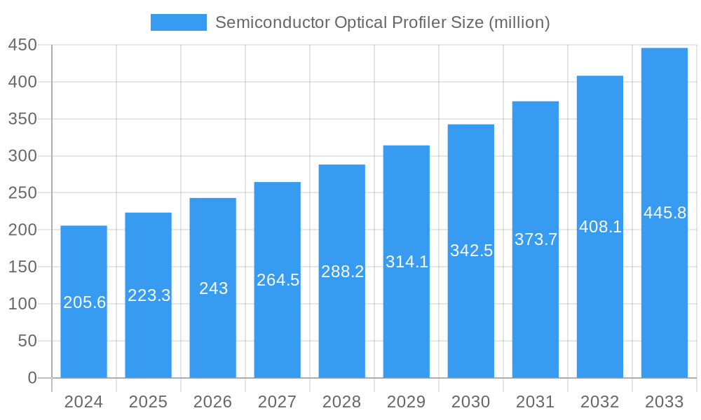
The global Semiconductor Optical Profiler market is experiencing robust growth, projected to reach an estimated $205.6 million in 2024. This expansion is fueled by the escalating demand for advanced semiconductor devices across various industries, including consumer electronics, automotive, and telecommunications. The intricate nature of modern semiconductor manufacturing and packaging necessitates highly precise metrology solutions, and optical profilers are at the forefront of this technological advancement. Their ability to provide non-contact, high-resolution surface topography measurements is critical for ensuring the quality and performance of microelectronic components. The market's projected compound annual growth rate (CAGR) of 8.8% from 2025 to 2033 signifies a sustained upward trajectory, driven by continuous innovation in chip design and the increasing complexity of manufacturing processes. Key applications within semiconductor manufacturing, such as wafer inspection and process control, alongside semiconductor packaging inspection for advanced packaging techniques, are primary growth areas.
Semiconductor Optical Profiler Market Size (In Million)
The market is further propelled by the increasing adoption of both desktop and portable optical profiler systems, catering to diverse operational needs within research laboratories, production floors, and field service environments. Major players like KLA, Bruker, and Keyence are actively investing in research and development to enhance profiler capabilities, offering faster acquisition times, higher accuracy, and expanded measurement ranges. Emerging trends include the integration of artificial intelligence and machine learning for automated data analysis and defect identification, as well as the development of multi-modal profilers that combine optical techniques with other metrology methods. While the market is largely driven by technological advancements, potential restraints could include the high initial investment cost of sophisticated profiler systems and the availability of alternative metrology solutions. However, the indispensable role of optical profilometry in achieving the stringent quality standards of the semiconductor industry is expected to outweigh these challenges, ensuring continued market expansion.
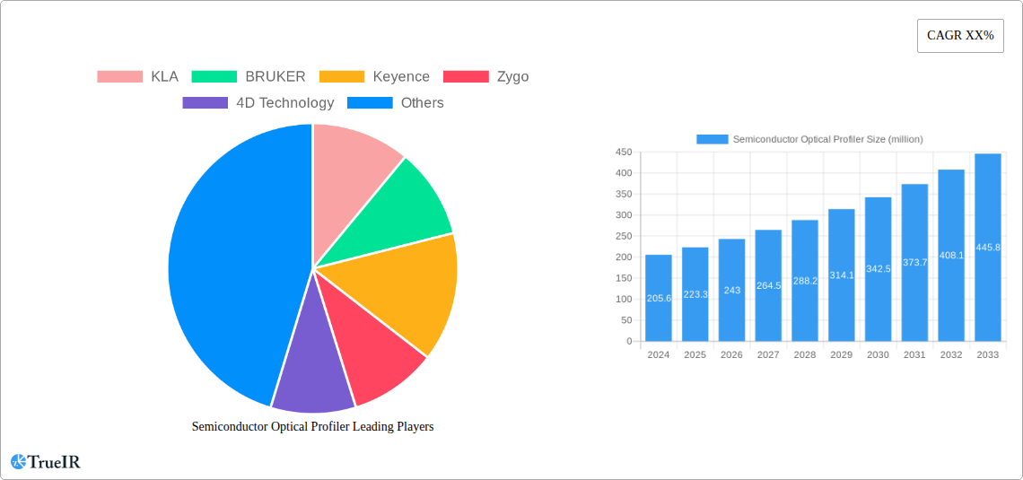
Semiconductor Optical Profiler Company Market Share
Semiconductor Optical Profiler Market Research Report: Unveiling Future Growth and Innovation
Gain unparalleled insights into the dynamic global Semiconductor Optical Profiler market with this comprehensive report. Covering the historical period of 2019-2024 and projecting growth through 2033, this study provides deep analysis of market structure, trends, dominant segments, product innovations, key drivers, challenges, and the competitive landscape. Essential for stakeholders seeking to navigate the rapidly evolving semiconductor industry, this report leverages high-volume keywords for maximum SEO impact and provides actionable intelligence for strategic decision-making.
Semiconductor Optical Profiler Market Structure & Competitive Landscape
The Semiconductor Optical Profiler market exhibits a XX% market concentration, with key players such as KLA, BRUKER, and Keyence dominating a significant portion of the market share. Innovation is primarily driven by the relentless demand for advanced semiconductor manufacturing processes, necessitating higher resolution, faster inspection, and non-contact metrology solutions. Regulatory impacts, while generally favorable due to the critical nature of semiconductor production, can influence adoption rates of new technologies. Product substitutes, such as scanning electron microscopes (SEMs) and atomic force microscopes (AFMs), exist but often lack the speed and scalability required for high-volume semiconductor production lines. End-user segmentation reveals a strong reliance on the Semiconductor Manufacturing segment, followed by Semiconductor Packaging Inspection. Mergers and acquisitions (M&A) are infrequent but impactful, with XX M&A deals valued at over XX million reported during the historical period, signaling consolidation and strategic expansion among leading firms. Key developments include the integration of AI and machine learning for enhanced defect detection and predictive maintenance, contributing to an estimated XX% year-over-year growth in advanced feature adoption.
Semiconductor Optical Profiler Market Trends & Opportunities
The global Semiconductor Optical Profiler market is poised for substantial expansion, projected to grow at a compound annual growth rate (CAGR) of XX% from the base year of 2025 to 2033. This robust growth is fueled by the burgeoning demand for advanced semiconductors across a myriad of applications, including artificial intelligence, 5G communication, and the Internet of Things (IoT). Technological shifts are at the forefront of this expansion, with a distinct trend towards higher resolution, faster acquisition speeds, and enhanced automation in optical profiling systems. Manufacturers are increasingly investing in non-contact metrology solutions to minimize wafer contamination and improve yield. Consumer preferences are evolving, demanding smaller, more powerful, and energy-efficient electronic devices, which directly translates into a need for more sophisticated semiconductor fabrication processes and, consequently, advanced inspection tools. The competitive dynamics are characterized by intense innovation, with established players continuously launching new products with improved capabilities to capture market share. Market penetration rates for advanced optical profilers are steadily increasing, particularly within leading semiconductor manufacturing hubs. The integration of interferometry, confocal microscopy, and structured light technologies is becoming standard, enabling the measurement of sub-nanometer surface features with unprecedented accuracy. Furthermore, the increasing complexity of advanced packaging techniques, such as 3D stacking and heterogeneous integration, is creating new opportunities for specialized optical profiling solutions capable of inspecting intricate 3D structures. The market is also witnessing a rise in demand for portable and desktop optical profilers, catering to smaller research and development facilities and on-site quality control needs. The ongoing miniaturization of transistors and the development of novel materials like 2D materials are driving the need for metrology tools that can characterize these ultra-thin layers and complex interfaces. Emerging applications in advanced lithography, such as extreme ultraviolet (EUV) lithography, are also a significant growth catalyst, requiring extremely precise surface characterization of masks and wafers. The market is expected to witness a surge in the adoption of AI-powered analytics, which will enable real-time defect classification and process optimization, further enhancing the efficiency and effectiveness of semiconductor manufacturing lines.
Dominant Markets & Segments in Semiconductor Optical Profiler
The Semiconductor Manufacturing application segment stands as the undisputed leader in the global Semiconductor Optical Profiler market, driven by the sheer volume and complexity of wafer fabrication processes. Within this segment, the inspection of critical features like gate oxides, metal interconnects, and lithographic patterns demands optical profiling solutions with sub-nanometer precision and high throughput. Countries with established and expanding semiconductor manufacturing infrastructure, such as South Korea, Taiwan, the United States, and China, represent the dominant regional markets.
Key Growth Drivers in Semiconductor Manufacturing Application:
- Global Demand for Advanced Semiconductors: The insatiable appetite for AI-powered devices, 5G infrastructure, and autonomous systems fuels continuous investment in cutting-edge semiconductor fabrication.
- Technological Advancements in Lithography: The relentless pursuit of smaller feature sizes, particularly with technologies like EUV lithography, necessitates extremely precise metrology for wafer and mask inspection.
- Yield Improvement Initiatives: Semiconductor manufacturers are under constant pressure to maximize wafer yields, making accurate and efficient surface profiling indispensable for defect detection and process control.
- Growing Investment in R&D: Significant global investments in semiconductor research and development lead to the adoption of advanced metrology tools for evaluating new materials and fabrication techniques.
The Semiconductor Packaging Inspection segment is experiencing rapid growth, driven by the increasing complexity of advanced packaging technologies. This includes 2.5D and 3D IC stacking, chiplet integration, and wafer-level packaging, all of which require meticulous inspection of interconnects, bumps, and underfill materials.
Key Growth Drivers in Semiconductor Packaging Inspection:
- Rise of Advanced Packaging: The industry's shift towards heterogeneous integration and multi-die solutions for enhanced performance and miniaturization.
- Miniaturization Trends: The need to inspect increasingly dense and intricate interconnects within smaller packaging footprints.
- Reliability and Quality Assurance: Ensuring the long-term reliability and performance of complex packaged devices through rigorous visual and dimensional inspection.
In terms of Types, the Desktop optical profiler segment holds a substantial market share due to its versatility, accuracy, and suitability for both R&D and in-line inspection on production floors. However, the Portable optical profiler segment is gaining traction, offering flexibility for on-site inspections and troubleshooting in diverse manufacturing environments. The market's trajectory indicates a continued dominance of desktop solutions, complemented by the growing niche for portable instrumentation.
Semiconductor Optical Profiler Product Analysis
Semiconductor optical profilers are at the forefront of metrology innovation, offering non-contact surface measurement with exceptional speed and accuracy. Key product advancements include the integration of multiple optical technologies, such as white light interferometry, confocal microscopy, and structured light, within a single platform to address a wider range of surface topographies and materials. These systems excel in characterizing critical dimensions, surface roughness, and defect analysis on semiconductor wafers, reticles, and packaged components. Their competitive advantage lies in their ability to provide detailed 3D surface maps, enabling rapid identification of process-related anomalies and ensuring adherence to stringent semiconductor manufacturing specifications.
Key Drivers, Barriers & Challenges in Semiconductor Optical Profiler
Key Drivers:
- Technological Advancements: The relentless drive for smaller semiconductor nodes and more complex architectures fuels the demand for higher-resolution, faster, and more automated optical profiling systems.
- Increasing Semiconductor Demand: The burgeoning global demand for advanced semiconductors in AI, IoT, and 5G applications directly translates into increased production volumes and metrology requirements.
- Government Initiatives and Investments: Favorable government policies and substantial investments in the semiconductor industry worldwide are accelerating market growth.
- Focus on Yield Improvement: Semiconductor manufacturers are prioritizing yield enhancement, making precise surface metrology crucial for defect detection and process control.
Key Barriers & Challenges:
- High Cost of Advanced Systems: Cutting-edge optical profilers represent a significant capital investment, posing a barrier for smaller players or R&D labs with limited budgets.
- Supply Chain Disruptions: Global supply chain vulnerabilities for critical components can impact manufacturing lead times and product availability.
- Complexity of Integration: Integrating new metrology solutions into existing semiconductor manufacturing workflows can be complex and time-consuming.
- Talent Shortage: A shortage of skilled personnel capable of operating and maintaining advanced optical profiling equipment can hinder adoption.
- Regulatory Hurdles: While generally favorable, evolving environmental and safety regulations can sometimes necessitate costly re-engineering of equipment.
Growth Drivers in the Semiconductor Optical Profiler Market
The Semiconductor Optical Profiler market's growth is primarily propelled by the escalating demand for advanced semiconductors fueled by rapid technological advancements in areas like AI, 5G, and the IoT. The continuous drive towards smaller semiconductor nodes and more intricate device architectures necessitates highly accurate, non-contact metrology solutions for process control and yield optimization. Government initiatives and significant global investments in the semiconductor industry are further accelerating this growth trajectory. Additionally, the increasing complexity of semiconductor packaging, including 3D integration and chiplet technology, is creating a strong demand for specialized optical profiling capabilities.
Challenges Impacting Semiconductor Optical Profiler Growth
Despite robust growth prospects, the Semiconductor Optical Profiler market faces several key challenges. The high capital expenditure associated with advanced optical profiling systems can be a significant barrier, particularly for emerging companies or smaller research facilities. Persistent global supply chain disruptions for critical components can lead to manufacturing delays and impact product availability. The intricate process of integrating new metrology solutions into established semiconductor manufacturing lines can also be complex and time-consuming, requiring substantial engineering effort. Furthermore, a persistent shortage of skilled professionals capable of operating and maintaining these sophisticated instruments presents an ongoing challenge.
Key Players Shaping the Semiconductor Optical Profiler Market
- KLA
- BRUKER
- Keyence
- Zygo
- 4D Technology
- HORIBA
- Mahr
- Sensofar
- Semilab
- CAMTEK
- Park Systems
- Taylor Hobson
- Skyverse Technology
- AMETEK
- Polytec
Significant Semiconductor Optical Profiler Industry Milestones
- 2019: Introduction of AI-powered defect detection algorithms in optical profilers, enhancing analysis speed and accuracy.
- 2020: Launch of ultra-high resolution optical profilometers capable of measuring features below 100 nanometers.
- 2021: Increased adoption of cloud-based data analytics for optical profiling systems, enabling remote monitoring and collaborative analysis.
- 2022: Development of novel illumination techniques for improved measurement of transparent and reflective materials.
- 2023: Emergence of integrated optical profiling solutions combining multiple metrology techniques for comprehensive wafer inspection.
- 2024: Significant advancements in portable optical profilers, offering enhanced mobility and on-site inspection capabilities for semiconductor manufacturing environments.
Future Outlook for Semiconductor Optical Profiler Market
The future of the Semiconductor Optical Profiler market is exceptionally bright, driven by the relentless pace of innovation in the semiconductor industry and the ever-increasing demand for high-performance electronic devices. Expect continued advancements in resolution, speed, and automation, with an emphasis on AI and machine learning for predictive analysis and process optimization. The growing complexity of semiconductor packaging will create significant opportunities for specialized optical profiling solutions. Strategic partnerships and acquisitions are likely to shape the competitive landscape, while the expansion into emerging markets and new application areas will fuel sustained growth, projecting an estimated market size of over XX billion by 2033.
Semiconductor Optical Profiler Segmentation
-
1. Application
- 1.1. Semiconductor Manufacturing
- 1.2. Semiconductor Packaging Inspection
-
2. Types
- 2.1. Desktop
- 2.2. Portable
Semiconductor Optical Profiler Segmentation By Geography
-
1. North America
- 1.1. United States
- 1.2. Canada
- 1.3. Mexico
-
2. South America
- 2.1. Brazil
- 2.2. Argentina
- 2.3. Rest of South America
-
3. Europe
- 3.1. United Kingdom
- 3.2. Germany
- 3.3. France
- 3.4. Italy
- 3.5. Spain
- 3.6. Russia
- 3.7. Benelux
- 3.8. Nordics
- 3.9. Rest of Europe
-
4. Middle East & Africa
- 4.1. Turkey
- 4.2. Israel
- 4.3. GCC
- 4.4. North Africa
- 4.5. South Africa
- 4.6. Rest of Middle East & Africa
-
5. Asia Pacific
- 5.1. China
- 5.2. India
- 5.3. Japan
- 5.4. South Korea
- 5.5. ASEAN
- 5.6. Oceania
- 5.7. Rest of Asia Pacific
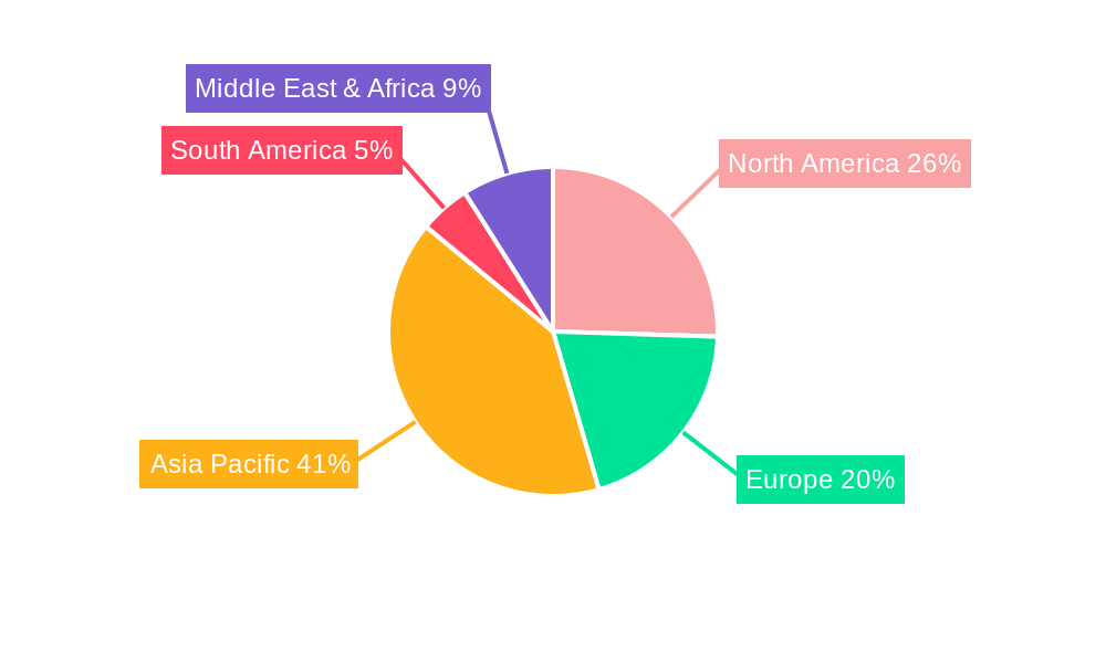
Semiconductor Optical Profiler Regional Market Share
Geographic Coverage of Semiconductor Optical Profiler
Semiconductor Optical Profiler REPORT HIGHLIGHTS
| Aspects | Details |
|---|---|
| Study Period | 2020-2034 |
| Base Year | 2025 |
| Estimated Year | 2026 |
| Forecast Period | 2026-2034 |
| Historical Period | 2020-2025 |
| Growth Rate | CAGR of 8.8% from 2020-2034 |
| Segmentation |
|
Table of Contents
- 1. Introduction
- 1.1. Research Scope
- 1.2. Market Segmentation
- 1.3. Research Methodology
- 1.4. Definitions and Assumptions
- 2. Executive Summary
- 2.1. Introduction
- 3. Market Dynamics
- 3.1. Introduction
- 3.2. Market Drivers
- 3.3. Market Restrains
- 3.4. Market Trends
- 4. Market Factor Analysis
- 4.1. Porters Five Forces
- 4.2. Supply/Value Chain
- 4.3. PESTEL analysis
- 4.4. Market Entropy
- 4.5. Patent/Trademark Analysis
- 5. Global Semiconductor Optical Profiler Analysis, Insights and Forecast, 2020-2032
- 5.1. Market Analysis, Insights and Forecast - by Application
- 5.1.1. Semiconductor Manufacturing
- 5.1.2. Semiconductor Packaging Inspection
- 5.2. Market Analysis, Insights and Forecast - by Types
- 5.2.1. Desktop
- 5.2.2. Portable
- 5.3. Market Analysis, Insights and Forecast - by Region
- 5.3.1. North America
- 5.3.2. South America
- 5.3.3. Europe
- 5.3.4. Middle East & Africa
- 5.3.5. Asia Pacific
- 5.1. Market Analysis, Insights and Forecast - by Application
- 6. North America Semiconductor Optical Profiler Analysis, Insights and Forecast, 2020-2032
- 6.1. Market Analysis, Insights and Forecast - by Application
- 6.1.1. Semiconductor Manufacturing
- 6.1.2. Semiconductor Packaging Inspection
- 6.2. Market Analysis, Insights and Forecast - by Types
- 6.2.1. Desktop
- 6.2.2. Portable
- 6.1. Market Analysis, Insights and Forecast - by Application
- 7. South America Semiconductor Optical Profiler Analysis, Insights and Forecast, 2020-2032
- 7.1. Market Analysis, Insights and Forecast - by Application
- 7.1.1. Semiconductor Manufacturing
- 7.1.2. Semiconductor Packaging Inspection
- 7.2. Market Analysis, Insights and Forecast - by Types
- 7.2.1. Desktop
- 7.2.2. Portable
- 7.1. Market Analysis, Insights and Forecast - by Application
- 8. Europe Semiconductor Optical Profiler Analysis, Insights and Forecast, 2020-2032
- 8.1. Market Analysis, Insights and Forecast - by Application
- 8.1.1. Semiconductor Manufacturing
- 8.1.2. Semiconductor Packaging Inspection
- 8.2. Market Analysis, Insights and Forecast - by Types
- 8.2.1. Desktop
- 8.2.2. Portable
- 8.1. Market Analysis, Insights and Forecast - by Application
- 9. Middle East & Africa Semiconductor Optical Profiler Analysis, Insights and Forecast, 2020-2032
- 9.1. Market Analysis, Insights and Forecast - by Application
- 9.1.1. Semiconductor Manufacturing
- 9.1.2. Semiconductor Packaging Inspection
- 9.2. Market Analysis, Insights and Forecast - by Types
- 9.2.1. Desktop
- 9.2.2. Portable
- 9.1. Market Analysis, Insights and Forecast - by Application
- 10. Asia Pacific Semiconductor Optical Profiler Analysis, Insights and Forecast, 2020-2032
- 10.1. Market Analysis, Insights and Forecast - by Application
- 10.1.1. Semiconductor Manufacturing
- 10.1.2. Semiconductor Packaging Inspection
- 10.2. Market Analysis, Insights and Forecast - by Types
- 10.2.1. Desktop
- 10.2.2. Portable
- 10.1. Market Analysis, Insights and Forecast - by Application
- 11. Competitive Analysis
- 11.1. Global Market Share Analysis 2025
- 11.2. Company Profiles
- 11.2.1 KLA
- 11.2.1.1. Overview
- 11.2.1.2. Products
- 11.2.1.3. SWOT Analysis
- 11.2.1.4. Recent Developments
- 11.2.1.5. Financials (Based on Availability)
- 11.2.2 BRUKER
- 11.2.2.1. Overview
- 11.2.2.2. Products
- 11.2.2.3. SWOT Analysis
- 11.2.2.4. Recent Developments
- 11.2.2.5. Financials (Based on Availability)
- 11.2.3 Keyence
- 11.2.3.1. Overview
- 11.2.3.2. Products
- 11.2.3.3. SWOT Analysis
- 11.2.3.4. Recent Developments
- 11.2.3.5. Financials (Based on Availability)
- 11.2.4 Zygo
- 11.2.4.1. Overview
- 11.2.4.2. Products
- 11.2.4.3. SWOT Analysis
- 11.2.4.4. Recent Developments
- 11.2.4.5. Financials (Based on Availability)
- 11.2.5 4D Technology
- 11.2.5.1. Overview
- 11.2.5.2. Products
- 11.2.5.3. SWOT Analysis
- 11.2.5.4. Recent Developments
- 11.2.5.5. Financials (Based on Availability)
- 11.2.6 HORIBA
- 11.2.6.1. Overview
- 11.2.6.2. Products
- 11.2.6.3. SWOT Analysis
- 11.2.6.4. Recent Developments
- 11.2.6.5. Financials (Based on Availability)
- 11.2.7 Mahr
- 11.2.7.1. Overview
- 11.2.7.2. Products
- 11.2.7.3. SWOT Analysis
- 11.2.7.4. Recent Developments
- 11.2.7.5. Financials (Based on Availability)
- 11.2.8 Sensofar
- 11.2.8.1. Overview
- 11.2.8.2. Products
- 11.2.8.3. SWOT Analysis
- 11.2.8.4. Recent Developments
- 11.2.8.5. Financials (Based on Availability)
- 11.2.9 Semilab
- 11.2.9.1. Overview
- 11.2.9.2. Products
- 11.2.9.3. SWOT Analysis
- 11.2.9.4. Recent Developments
- 11.2.9.5. Financials (Based on Availability)
- 11.2.10 CAMTEK
- 11.2.10.1. Overview
- 11.2.10.2. Products
- 11.2.10.3. SWOT Analysis
- 11.2.10.4. Recent Developments
- 11.2.10.5. Financials (Based on Availability)
- 11.2.11 Park Systems
- 11.2.11.1. Overview
- 11.2.11.2. Products
- 11.2.11.3. SWOT Analysis
- 11.2.11.4. Recent Developments
- 11.2.11.5. Financials (Based on Availability)
- 11.2.12 Taylor Hobson
- 11.2.12.1. Overview
- 11.2.12.2. Products
- 11.2.12.3. SWOT Analysis
- 11.2.12.4. Recent Developments
- 11.2.12.5. Financials (Based on Availability)
- 11.2.13 Skyverse Technology
- 11.2.13.1. Overview
- 11.2.13.2. Products
- 11.2.13.3. SWOT Analysis
- 11.2.13.4. Recent Developments
- 11.2.13.5. Financials (Based on Availability)
- 11.2.14 AMETEK
- 11.2.14.1. Overview
- 11.2.14.2. Products
- 11.2.14.3. SWOT Analysis
- 11.2.14.4. Recent Developments
- 11.2.14.5. Financials (Based on Availability)
- 11.2.15 Polytec
- 11.2.15.1. Overview
- 11.2.15.2. Products
- 11.2.15.3. SWOT Analysis
- 11.2.15.4. Recent Developments
- 11.2.15.5. Financials (Based on Availability)
- 11.2.1 KLA
List of Figures
- Figure 1: Global Semiconductor Optical Profiler Revenue Breakdown (undefined, %) by Region 2025 & 2033
- Figure 2: North America Semiconductor Optical Profiler Revenue (undefined), by Application 2025 & 2033
- Figure 3: North America Semiconductor Optical Profiler Revenue Share (%), by Application 2025 & 2033
- Figure 4: North America Semiconductor Optical Profiler Revenue (undefined), by Types 2025 & 2033
- Figure 5: North America Semiconductor Optical Profiler Revenue Share (%), by Types 2025 & 2033
- Figure 6: North America Semiconductor Optical Profiler Revenue (undefined), by Country 2025 & 2033
- Figure 7: North America Semiconductor Optical Profiler Revenue Share (%), by Country 2025 & 2033
- Figure 8: South America Semiconductor Optical Profiler Revenue (undefined), by Application 2025 & 2033
- Figure 9: South America Semiconductor Optical Profiler Revenue Share (%), by Application 2025 & 2033
- Figure 10: South America Semiconductor Optical Profiler Revenue (undefined), by Types 2025 & 2033
- Figure 11: South America Semiconductor Optical Profiler Revenue Share (%), by Types 2025 & 2033
- Figure 12: South America Semiconductor Optical Profiler Revenue (undefined), by Country 2025 & 2033
- Figure 13: South America Semiconductor Optical Profiler Revenue Share (%), by Country 2025 & 2033
- Figure 14: Europe Semiconductor Optical Profiler Revenue (undefined), by Application 2025 & 2033
- Figure 15: Europe Semiconductor Optical Profiler Revenue Share (%), by Application 2025 & 2033
- Figure 16: Europe Semiconductor Optical Profiler Revenue (undefined), by Types 2025 & 2033
- Figure 17: Europe Semiconductor Optical Profiler Revenue Share (%), by Types 2025 & 2033
- Figure 18: Europe Semiconductor Optical Profiler Revenue (undefined), by Country 2025 & 2033
- Figure 19: Europe Semiconductor Optical Profiler Revenue Share (%), by Country 2025 & 2033
- Figure 20: Middle East & Africa Semiconductor Optical Profiler Revenue (undefined), by Application 2025 & 2033
- Figure 21: Middle East & Africa Semiconductor Optical Profiler Revenue Share (%), by Application 2025 & 2033
- Figure 22: Middle East & Africa Semiconductor Optical Profiler Revenue (undefined), by Types 2025 & 2033
- Figure 23: Middle East & Africa Semiconductor Optical Profiler Revenue Share (%), by Types 2025 & 2033
- Figure 24: Middle East & Africa Semiconductor Optical Profiler Revenue (undefined), by Country 2025 & 2033
- Figure 25: Middle East & Africa Semiconductor Optical Profiler Revenue Share (%), by Country 2025 & 2033
- Figure 26: Asia Pacific Semiconductor Optical Profiler Revenue (undefined), by Application 2025 & 2033
- Figure 27: Asia Pacific Semiconductor Optical Profiler Revenue Share (%), by Application 2025 & 2033
- Figure 28: Asia Pacific Semiconductor Optical Profiler Revenue (undefined), by Types 2025 & 2033
- Figure 29: Asia Pacific Semiconductor Optical Profiler Revenue Share (%), by Types 2025 & 2033
- Figure 30: Asia Pacific Semiconductor Optical Profiler Revenue (undefined), by Country 2025 & 2033
- Figure 31: Asia Pacific Semiconductor Optical Profiler Revenue Share (%), by Country 2025 & 2033
List of Tables
- Table 1: Global Semiconductor Optical Profiler Revenue undefined Forecast, by Application 2020 & 2033
- Table 2: Global Semiconductor Optical Profiler Revenue undefined Forecast, by Types 2020 & 2033
- Table 3: Global Semiconductor Optical Profiler Revenue undefined Forecast, by Region 2020 & 2033
- Table 4: Global Semiconductor Optical Profiler Revenue undefined Forecast, by Application 2020 & 2033
- Table 5: Global Semiconductor Optical Profiler Revenue undefined Forecast, by Types 2020 & 2033
- Table 6: Global Semiconductor Optical Profiler Revenue undefined Forecast, by Country 2020 & 2033
- Table 7: United States Semiconductor Optical Profiler Revenue (undefined) Forecast, by Application 2020 & 2033
- Table 8: Canada Semiconductor Optical Profiler Revenue (undefined) Forecast, by Application 2020 & 2033
- Table 9: Mexico Semiconductor Optical Profiler Revenue (undefined) Forecast, by Application 2020 & 2033
- Table 10: Global Semiconductor Optical Profiler Revenue undefined Forecast, by Application 2020 & 2033
- Table 11: Global Semiconductor Optical Profiler Revenue undefined Forecast, by Types 2020 & 2033
- Table 12: Global Semiconductor Optical Profiler Revenue undefined Forecast, by Country 2020 & 2033
- Table 13: Brazil Semiconductor Optical Profiler Revenue (undefined) Forecast, by Application 2020 & 2033
- Table 14: Argentina Semiconductor Optical Profiler Revenue (undefined) Forecast, by Application 2020 & 2033
- Table 15: Rest of South America Semiconductor Optical Profiler Revenue (undefined) Forecast, by Application 2020 & 2033
- Table 16: Global Semiconductor Optical Profiler Revenue undefined Forecast, by Application 2020 & 2033
- Table 17: Global Semiconductor Optical Profiler Revenue undefined Forecast, by Types 2020 & 2033
- Table 18: Global Semiconductor Optical Profiler Revenue undefined Forecast, by Country 2020 & 2033
- Table 19: United Kingdom Semiconductor Optical Profiler Revenue (undefined) Forecast, by Application 2020 & 2033
- Table 20: Germany Semiconductor Optical Profiler Revenue (undefined) Forecast, by Application 2020 & 2033
- Table 21: France Semiconductor Optical Profiler Revenue (undefined) Forecast, by Application 2020 & 2033
- Table 22: Italy Semiconductor Optical Profiler Revenue (undefined) Forecast, by Application 2020 & 2033
- Table 23: Spain Semiconductor Optical Profiler Revenue (undefined) Forecast, by Application 2020 & 2033
- Table 24: Russia Semiconductor Optical Profiler Revenue (undefined) Forecast, by Application 2020 & 2033
- Table 25: Benelux Semiconductor Optical Profiler Revenue (undefined) Forecast, by Application 2020 & 2033
- Table 26: Nordics Semiconductor Optical Profiler Revenue (undefined) Forecast, by Application 2020 & 2033
- Table 27: Rest of Europe Semiconductor Optical Profiler Revenue (undefined) Forecast, by Application 2020 & 2033
- Table 28: Global Semiconductor Optical Profiler Revenue undefined Forecast, by Application 2020 & 2033
- Table 29: Global Semiconductor Optical Profiler Revenue undefined Forecast, by Types 2020 & 2033
- Table 30: Global Semiconductor Optical Profiler Revenue undefined Forecast, by Country 2020 & 2033
- Table 31: Turkey Semiconductor Optical Profiler Revenue (undefined) Forecast, by Application 2020 & 2033
- Table 32: Israel Semiconductor Optical Profiler Revenue (undefined) Forecast, by Application 2020 & 2033
- Table 33: GCC Semiconductor Optical Profiler Revenue (undefined) Forecast, by Application 2020 & 2033
- Table 34: North Africa Semiconductor Optical Profiler Revenue (undefined) Forecast, by Application 2020 & 2033
- Table 35: South Africa Semiconductor Optical Profiler Revenue (undefined) Forecast, by Application 2020 & 2033
- Table 36: Rest of Middle East & Africa Semiconductor Optical Profiler Revenue (undefined) Forecast, by Application 2020 & 2033
- Table 37: Global Semiconductor Optical Profiler Revenue undefined Forecast, by Application 2020 & 2033
- Table 38: Global Semiconductor Optical Profiler Revenue undefined Forecast, by Types 2020 & 2033
- Table 39: Global Semiconductor Optical Profiler Revenue undefined Forecast, by Country 2020 & 2033
- Table 40: China Semiconductor Optical Profiler Revenue (undefined) Forecast, by Application 2020 & 2033
- Table 41: India Semiconductor Optical Profiler Revenue (undefined) Forecast, by Application 2020 & 2033
- Table 42: Japan Semiconductor Optical Profiler Revenue (undefined) Forecast, by Application 2020 & 2033
- Table 43: South Korea Semiconductor Optical Profiler Revenue (undefined) Forecast, by Application 2020 & 2033
- Table 44: ASEAN Semiconductor Optical Profiler Revenue (undefined) Forecast, by Application 2020 & 2033
- Table 45: Oceania Semiconductor Optical Profiler Revenue (undefined) Forecast, by Application 2020 & 2033
- Table 46: Rest of Asia Pacific Semiconductor Optical Profiler Revenue (undefined) Forecast, by Application 2020 & 2033
Frequently Asked Questions
1. What is the projected Compound Annual Growth Rate (CAGR) of the Semiconductor Optical Profiler?
The projected CAGR is approximately 8.8%.
2. Which companies are prominent players in the Semiconductor Optical Profiler?
Key companies in the market include KLA, BRUKER, Keyence, Zygo, 4D Technology, HORIBA, Mahr, Sensofar, Semilab, CAMTEK, Park Systems, Taylor Hobson, Skyverse Technology, AMETEK, Polytec.
3. What are the main segments of the Semiconductor Optical Profiler?
The market segments include Application, Types.
4. Can you provide details about the market size?
The market size is estimated to be USD XXX N/A as of 2022.
5. What are some drivers contributing to market growth?
N/A
6. What are the notable trends driving market growth?
N/A
7. Are there any restraints impacting market growth?
N/A
8. Can you provide examples of recent developments in the market?
N/A
9. What pricing options are available for accessing the report?
Pricing options include single-user, multi-user, and enterprise licenses priced at USD 4900.00, USD 7350.00, and USD 9800.00 respectively.
10. Is the market size provided in terms of value or volume?
The market size is provided in terms of value, measured in N/A.
11. Are there any specific market keywords associated with the report?
Yes, the market keyword associated with the report is "Semiconductor Optical Profiler," which aids in identifying and referencing the specific market segment covered.
12. How do I determine which pricing option suits my needs best?
The pricing options vary based on user requirements and access needs. Individual users may opt for single-user licenses, while businesses requiring broader access may choose multi-user or enterprise licenses for cost-effective access to the report.
13. Are there any additional resources or data provided in the Semiconductor Optical Profiler report?
While the report offers comprehensive insights, it's advisable to review the specific contents or supplementary materials provided to ascertain if additional resources or data are available.
14. How can I stay updated on further developments or reports in the Semiconductor Optical Profiler?
To stay informed about further developments, trends, and reports in the Semiconductor Optical Profiler, consider subscribing to industry newsletters, following relevant companies and organizations, or regularly checking reputable industry news sources and publications.
Methodology
Step 1 - Identification of Relevant Samples Size from Population Database


Step 2 - Approaches for Defining Global Market Size (Value, Volume* & Price*)

Note*: In applicable scenarios
Step 3 - Data Sources
Primary Research
- Web Analytics
- Survey Reports
- Research Institute
- Latest Research Reports
- Opinion Leaders
Secondary Research
- Annual Reports
- White Paper
- Latest Press Release
- Industry Association
- Paid Database
- Investor Presentations

Step 4 - Data Triangulation
Involves using different sources of information in order to increase the validity of a study
These sources are likely to be stakeholders in a program - participants, other researchers, program staff, other community members, and so on.
Then we put all data in single framework & apply various statistical tools to find out the dynamic on the market.
During the analysis stage, feedback from the stakeholder groups would be compared to determine areas of agreement as well as areas of divergence