

Key Insights
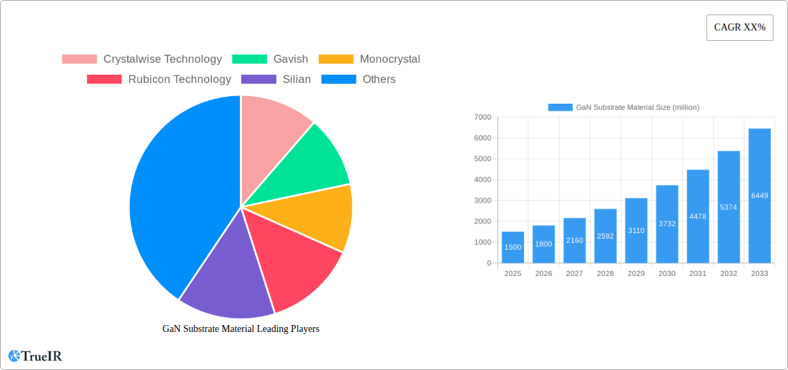
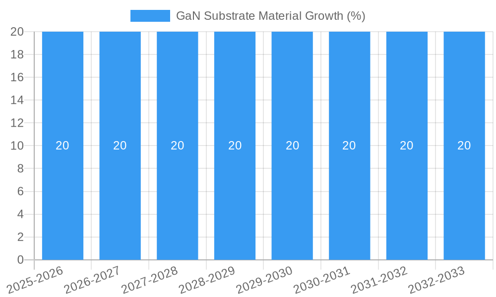
The GaN substrate material market is poised for substantial growth, projected to reach an estimated market size of approximately $1,500 million by 2025, with a robust Compound Annual Growth Rate (CAGR) of around 20% expected through 2033. This expansion is primarily fueled by the escalating demand for advanced electronic components across a multitude of industries. The burgeoning application of Gallium Nitride (GaN) in high-efficiency Light Emitting Diodes (LEDs) for lighting and displays, Radio Frequency Integrated Circuits (RFICs) essential for 5G infrastructure and advanced telecommunications, and high-performance Laser Diodes for optical communications and industrial applications are significant growth drivers. Furthermore, ongoing innovation in semiconductor technology and the increasing adoption of power electronics for energy efficiency are creating a fertile ground for GaN substrates. The inherent properties of GaN, such as its high bandgap, superior thermal conductivity, and resistance to high temperatures and voltages, make it an indispensable material for next-generation devices.
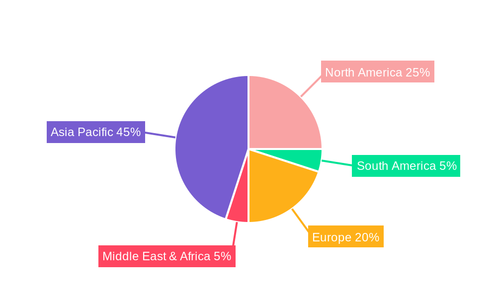
The market landscape is characterized by a dynamic interplay of technological advancements and strategic collaborations among leading global players like Mitsubishi Chemical, Sumitomo Electric, and Shin-Etsu, alongside emerging innovators such as Crystalwise Technology and Yuanliang Technology. While the market is experiencing strong upward momentum, certain restraints, such as the high manufacturing costs associated with GaN substrate production and the availability of alternative materials in specific applications, warrant careful consideration. However, the relentless pursuit of enhanced performance, miniaturization, and energy efficiency in electronic devices continues to drive research and development, leading to improved manufacturing processes and cost reductions. The market is segmented into key applications including Light Emitting Diode (LED), Radio Frequency Integrated Circuit (RFIC), and Laser Diode, with Sapphire Blue, Si, SiC, and GaN representing critical substrate types. Geographically, the Asia Pacific region, led by China and Japan, is expected to dominate the market due to its strong manufacturing base and significant investments in advanced electronics, followed by North America and Europe.
GaN Substrate Material Market Structure & Competitive Landscape
The GaN substrate material market is characterized by a moderately concentrated competitive landscape, with key players investing heavily in research and development to drive innovation. The market's evolution is being shaped by advancements in epitaxy techniques, wafer manufacturing processes, and the increasing demand for high-performance electronic and optoelectronic devices. Regulatory influences, particularly concerning material standards and environmental impact, play a crucial role in shaping manufacturing practices and market entry barriers. The presence of potential product substitutes, such as advanced silicon or other wide-bandgap semiconductor materials, necessitates continuous innovation and cost optimization by GaN substrate manufacturers. End-user segmentation reveals a strong reliance on the RFIC and LED sectors, with emerging applications in power electronics and high-power laser diodes also contributing to market diversification. Mergers and acquisitions (M&A) activity, while not dominant, is present, indicating a strategic consolidation trend among companies seeking to expand their product portfolios and market reach. The total M&A volume in the historical period (2019-2024) is estimated at over one million dollars, reflecting strategic partnerships and small-scale acquisitions aimed at bolstering technological capabilities. Concentration ratios, particularly in the high-volume GaN-on-sapphire segment, indicate a significant market share held by the top few players, exceeding 60% in some sub-segments.
GaN Substrate Material Market Trends & Opportunities
The GaN substrate material market is experiencing robust growth, projected to reach a market size exceeding one million dollars by the end of the forecast period. This expansion is fueled by a confluence of technological advancements and burgeoning application demands across critical industries. The increasing adoption of GaN in Radio Frequency Integrated Circuits (RFICs) for advanced wireless communication technologies, including 5G infrastructure and next-generation mobile devices, is a primary growth driver. The superior performance characteristics of GaN, such as high electron mobility and breakdown voltage, enable smaller, more power-efficient, and faster RF components compared to traditional silicon-based solutions. This technological shift presents significant opportunities for substrate manufacturers to develop high-quality, defect-free GaN wafers tailored for these demanding applications.
Furthermore, the Light Emitting Diode (LED) segment continues to be a significant contributor to market growth. GaN-based LEDs are essential for energy-efficient lighting solutions, display technologies, and automotive lighting. The ongoing demand for brighter, more energy-efficient, and longer-lasting LEDs across residential, commercial, and industrial sectors ensures a consistent market for GaN substrates. The development of novel LED architectures and enhanced optical performance further accentuates this trend.
The market is also witnessing a growing interest in GaN for power electronics applications, such as high-efficiency power converters and electric vehicle charging infrastructure. GaN's ability to handle higher voltages and frequencies with lower power loss makes it an attractive alternative to silicon carbide (SiC) and silicon in certain applications, presenting a substantial growth avenue. Laser diode applications, particularly in areas like industrial cutting, medical devices, and optical sensing, are also contributing to market expansion, albeit with a more niche but high-value focus.
Consumer preferences are increasingly leaning towards devices that offer enhanced performance, energy efficiency, and miniaturization, all of which are core benefits derived from GaN-based technologies. This shift directly translates into a higher demand for advanced GaN substrates. The competitive dynamics are characterized by ongoing innovation in epitaxy, with companies striving to reduce defect densities, improve wafer uniformity, and develop cost-effective manufacturing processes. The market penetration rate for GaN substrates in emerging RF and power applications is steadily increasing, signaling a significant shift away from traditional semiconductor materials. The Compound Annual Growth Rate (CAGR) for the GaN substrate material market is estimated to be in the range of 10-15% during the forecast period, reflecting its strong growth trajectory.
Dominant Markets & Segments in GaN Substrate Material
The GaN substrate material market is predominantly driven by the Asia-Pacific region, with China and South Korea emerging as leading countries in both production and consumption. This dominance is attributable to the substantial manufacturing base for electronic components and consumer devices within these nations, coupled with significant government support for semiconductor industry development. The Application segment of Radio Frequency Integrated Circuits (RFIC) is a major area of market dominance, largely propelled by the global rollout of 5G infrastructure. The inherent advantages of GaN, including high frequency operation, power efficiency, and reduced size, make it indispensable for advanced base stations, mobile devices, and radar systems. The continuous upgrade cycles in telecommunications and defense sectors further solidify RFIC's leading position.
Within the Types of GaN substrate materials, GaN itself, particularly when grown on various substrates like sapphire or silicon carbide, holds the largest market share. However, the report also considers Sapphire Blue as a critical substrate for certain GaN-on-sapphire applications, especially in LEDs, which are also a significant application segment.
Application: Light Emitting Diode (LED): This segment, while mature in some aspects, continues to be a strong contributor due to ongoing demand for energy-efficient lighting, advanced display technologies (e.g., MicroLEDs), and automotive lighting. Government initiatives promoting energy conservation and the adoption of LED lighting globally bolster this segment. The infrastructure development in emerging economies and the continuous innovation in LED performance and form factors are key growth drivers.
Application: Radio Frequency Integrated Circuit (RFIC): This is the most dynamic and rapidly growing application segment for GaN substrates. The insatiable demand for higher bandwidth, faster data speeds, and increased connectivity in smartphones, base stations, and defense systems directly fuels the need for high-performance GaN RF devices. Technological advancements in miniaturization and power efficiency are critical here.
Type: GaN: As the primary material for advanced semiconductor devices, GaN substrates (both native and heteroepitaxial) are crucial across all leading applications. The ongoing refinement of GaN growth techniques, aiming for higher crystal quality and lower defect density, is critical for unlocking the full potential of GaN devices.
Regional Dominance (Asia-Pacific): The extensive manufacturing ecosystem for electronics, coupled with supportive government policies and substantial R&D investments in countries like China, South Korea, and Japan, positions Asia-Pacific as the dominant market. The region's robust demand for consumer electronics and telecommunications infrastructure is a primary driver.
The Laser Diode application, while smaller in volume, represents a high-value segment with significant growth potential driven by advancements in industrial, medical, and optical communication technologies. The Others category, encompassing emerging applications like power electronics and sensors, is poised for substantial future growth as GaN's unique properties are further explored and leveraged.
GaN Substrate Material Product Analysis
GaN substrate materials are at the forefront of technological innovation, enabling next-generation electronic and optoelectronic devices. Key product innovations focus on reducing crystalline defects, improving wafer uniformity, and achieving larger wafer diameters for increased manufacturing efficiency and cost reduction. These advancements directly translate into enhanced performance characteristics for GaN-based components, such as higher power handling capabilities, improved efficiency, and extended device lifetimes. Applications span across high-performance RF power amplifiers for 5G communication, energy-efficient LED lighting, advanced laser diodes for industrial and medical use, and power electronics for electric vehicles and renewable energy systems. The competitive advantage of GaN substrates lies in their ability to deliver superior performance in high-frequency, high-temperature, and high-power environments, surpassing traditional semiconductor materials like silicon.
Key Drivers, Barriers & Challenges in GaN Substrate Material
The GaN substrate material market is propelled by several key drivers. Technologically, the unparalleled performance characteristics of GaN, including high breakdown voltage, high electron mobility, and excellent thermal conductivity, are critical for enabling high-frequency, high-power, and energy-efficient devices. The burgeoning demand for 5G infrastructure, advanced consumer electronics, and electric vehicles significantly fuels this demand. Economic factors, such as increasing energy efficiency mandates and the drive for miniaturization in electronic devices, also act as powerful catalysts. Policy-driven factors, including government initiatives supporting domestic semiconductor manufacturing and R&D investments in next-generation technologies, further bolster market growth. For example, substantial government incentives for 5G deployment globally directly translate into increased demand for GaN RF components.
However, significant challenges and restraints impede market growth. Supply chain complexities, particularly in sourcing high-purity raw materials and ensuring consistent quality across wafer manufacturing, pose a substantial hurdle. Regulatory hurdles, although less prominent, can emerge regarding environmental compliance and material standards for specific applications. Competitive pressures from alternative wide-bandgap semiconductor materials like Silicon Carbide (SiC) in certain high-power applications necessitate continuous innovation and cost competitiveness. The high cost of GaN substrate manufacturing, especially for larger wafer diameters and low defect density, remains a primary barrier to widespread adoption in cost-sensitive applications. For instance, the cost per wafer can be over one million dollars for advanced configurations.
Growth Drivers in the GaN Substrate Material Market
The growth of the GaN substrate material market is primarily driven by technological advancements that unlock superior device performance. The insatiable demand for faster, more efficient, and smaller electronic devices, particularly in the telecommunications (5G and beyond) and consumer electronics sectors, is a fundamental economic driver. Government investments in strategic industries, such as semiconductors and renewable energy, coupled with supportive policies promoting innovation and domestic production, create a favorable environment for market expansion. For instance, initiatives focused on energy efficiency and the electrification of transportation are creating substantial opportunities for GaN-based power electronics. The continuous improvement in GaN epitaxy techniques, leading to higher crystal quality and reduced manufacturing costs, also plays a crucial role in widening market adoption.
Challenges Impacting GaN Substrate Material Growth
Despite its promising outlook, the GaN substrate material market faces several critical challenges. The high cost of manufacturing GaN substrates, particularly for high-quality, large-diameter wafers, remains a significant barrier to entry for some applications. Supply chain vulnerabilities, including the availability of essential raw materials and specialized manufacturing equipment, can lead to production delays and increased costs. Regulatory complexities related to environmental impact and material sourcing, though less prominent currently, could evolve and necessitate adjustments in manufacturing processes. Intense competitive pressures from established silicon technology and emerging SiC solutions in specific market segments require constant innovation and cost optimization to maintain market share. For example, the cost of producing a 6-inch GaN wafer can exceed one million dollars, impacting broader adoption.
Key Players Shaping the GaN Substrate Material Market
- Crystalwise Technology
- Gavish
- Monocrystal
- Rubicon Technology
- Silian
- Shanxi Huajing Hengji New Materials
- Yuanliang Technology
- Huacan Optoelectronics Co.,Ltd.
- Sanan Optoelectronics Co.,Ltd.
- Precision Micro-Optics
- Adamant Namiki
- Mitsubishi Chemical
- Sumitomo Electric
- Hitachi
- Shin-Etsu
- Fuji Electric
Significant GaN Substrate Material Industry Milestones
- 2019: Significant advancements in GaN-on-Si epitaxy techniques reported, promising lower costs for GaN substrates.
- 2020: Key players announce investments exceeding one million dollars in R&D for higher-quality GaN substrates.
- 2021: Increased adoption of GaN substrates in 5G infrastructure components drives market expansion.
- 2022: Development of larger diameter GaN wafers (e.g., 8-inch) by leading manufacturers, improving scalability and cost-effectiveness.
- 2023: Emerging applications in electric vehicle power electronics gain traction, boosting demand for high-performance GaN substrates.
- 2024: Continued progress in reducing defect densities in GaN substrates, enhancing device reliability and performance.
Future Outlook for GaN Substrate Material Market
The future outlook for the GaN substrate material market is exceptionally bright, driven by sustained technological innovation and expanding application frontiers. Strategic opportunities lie in the continued growth of 5G and future wireless communication standards, the burgeoning electric vehicle market, and the increasing demand for high-efficiency power electronics and advanced lighting solutions. The ongoing development of cost-effective manufacturing processes, such as advancements in GaN-on-Si technology and larger wafer diameter production, will be crucial for broadening market penetration. Market potential is further amplified by the exploration of novel applications in areas like high-frequency radar systems, quantum computing, and advanced sensing technologies. Investments in research and development aimed at improving material quality and reducing production costs are expected to be key catalysts for sustained market growth over the next decade, with the market size projected to exceed one million dollars.
GaN Substrate Material Segmentation
-
1. Application
- 1.1. Light Emitting Diode (LED)
- 1.2. Radio Frequency Integrated Circuit (RFIC)
- 1.3. Laser Diode
- 1.4. Others
-
2. Types
- 2.1. Sapphire Blue
- 2.2. Si
- 2.3. SiC
- 2.4. GaN
GaN Substrate Material Segmentation By Geography
-
1. North America
- 1.1. United States
- 1.2. Canada
- 1.3. Mexico
-
2. South America
- 2.1. Brazil
- 2.2. Argentina
- 2.3. Rest of South America
-
3. Europe
- 3.1. United Kingdom
- 3.2. Germany
- 3.3. France
- 3.4. Italy
- 3.5. Spain
- 3.6. Russia
- 3.7. Benelux
- 3.8. Nordics
- 3.9. Rest of Europe
-
4. Middle East & Africa
- 4.1. Turkey
- 4.2. Israel
- 4.3. GCC
- 4.4. North Africa
- 4.5. South Africa
- 4.6. Rest of Middle East & Africa
-
5. Asia Pacific
- 5.1. China
- 5.2. India
- 5.3. Japan
- 5.4. South Korea
- 5.5. ASEAN
- 5.6. Oceania
- 5.7. Rest of Asia Pacific
GaN Substrate Material REPORT HIGHLIGHTS
| Aspects | Details |
|---|---|
| Study Period | 2019-2033 |
| Base Year | 2024 |
| Estimated Year | 2025 |
| Forecast Period | 2025-2033 |
| Historical Period | 2019-2024 |
| Growth Rate | CAGR of XX% from 2019-2033 |
| Segmentation |
|
Table of Contents
- 1. Introduction
- 1.1. Research Scope
- 1.2. Market Segmentation
- 1.3. Research Methodology
- 1.4. Definitions and Assumptions
- 2. Executive Summary
- 2.1. Introduction
- 3. Market Dynamics
- 3.1. Introduction
- 3.2. Market Drivers
- 3.3. Market Restrains
- 3.4. Market Trends
- 4. Market Factor Analysis
- 4.1. Porters Five Forces
- 4.2. Supply/Value Chain
- 4.3. PESTEL analysis
- 4.4. Market Entropy
- 4.5. Patent/Trademark Analysis
- 5. Global GaN Substrate Material Analysis, Insights and Forecast, 2019-2031
- 5.1. Market Analysis, Insights and Forecast - by Application
- 5.1.1. Light Emitting Diode (LED)
- 5.1.2. Radio Frequency Integrated Circuit (RFIC)
- 5.1.3. Laser Diode
- 5.1.4. Others
- 5.2. Market Analysis, Insights and Forecast - by Types
- 5.2.1. Sapphire Blue
- 5.2.2. Si
- 5.2.3. SiC
- 5.2.4. GaN
- 5.3. Market Analysis, Insights and Forecast - by Region
- 5.3.1. North America
- 5.3.2. South America
- 5.3.3. Europe
- 5.3.4. Middle East & Africa
- 5.3.5. Asia Pacific
- 5.1. Market Analysis, Insights and Forecast - by Application
- 6. North America GaN Substrate Material Analysis, Insights and Forecast, 2019-2031
- 6.1. Market Analysis, Insights and Forecast - by Application
- 6.1.1. Light Emitting Diode (LED)
- 6.1.2. Radio Frequency Integrated Circuit (RFIC)
- 6.1.3. Laser Diode
- 6.1.4. Others
- 6.2. Market Analysis, Insights and Forecast - by Types
- 6.2.1. Sapphire Blue
- 6.2.2. Si
- 6.2.3. SiC
- 6.2.4. GaN
- 6.1. Market Analysis, Insights and Forecast - by Application
- 7. South America GaN Substrate Material Analysis, Insights and Forecast, 2019-2031
- 7.1. Market Analysis, Insights and Forecast - by Application
- 7.1.1. Light Emitting Diode (LED)
- 7.1.2. Radio Frequency Integrated Circuit (RFIC)
- 7.1.3. Laser Diode
- 7.1.4. Others
- 7.2. Market Analysis, Insights and Forecast - by Types
- 7.2.1. Sapphire Blue
- 7.2.2. Si
- 7.2.3. SiC
- 7.2.4. GaN
- 7.1. Market Analysis, Insights and Forecast - by Application
- 8. Europe GaN Substrate Material Analysis, Insights and Forecast, 2019-2031
- 8.1. Market Analysis, Insights and Forecast - by Application
- 8.1.1. Light Emitting Diode (LED)
- 8.1.2. Radio Frequency Integrated Circuit (RFIC)
- 8.1.3. Laser Diode
- 8.1.4. Others
- 8.2. Market Analysis, Insights and Forecast - by Types
- 8.2.1. Sapphire Blue
- 8.2.2. Si
- 8.2.3. SiC
- 8.2.4. GaN
- 8.1. Market Analysis, Insights and Forecast - by Application
- 9. Middle East & Africa GaN Substrate Material Analysis, Insights and Forecast, 2019-2031
- 9.1. Market Analysis, Insights and Forecast - by Application
- 9.1.1. Light Emitting Diode (LED)
- 9.1.2. Radio Frequency Integrated Circuit (RFIC)
- 9.1.3. Laser Diode
- 9.1.4. Others
- 9.2. Market Analysis, Insights and Forecast - by Types
- 9.2.1. Sapphire Blue
- 9.2.2. Si
- 9.2.3. SiC
- 9.2.4. GaN
- 9.1. Market Analysis, Insights and Forecast - by Application
- 10. Asia Pacific GaN Substrate Material Analysis, Insights and Forecast, 2019-2031
- 10.1. Market Analysis, Insights and Forecast - by Application
- 10.1.1. Light Emitting Diode (LED)
- 10.1.2. Radio Frequency Integrated Circuit (RFIC)
- 10.1.3. Laser Diode
- 10.1.4. Others
- 10.2. Market Analysis, Insights and Forecast - by Types
- 10.2.1. Sapphire Blue
- 10.2.2. Si
- 10.2.3. SiC
- 10.2.4. GaN
- 10.1. Market Analysis, Insights and Forecast - by Application
- 11. Competitive Analysis
- 11.1. Global Market Share Analysis 2024
- 11.2. Company Profiles
- 11.2.1 Crystalwise Technology
- 11.2.1.1. Overview
- 11.2.1.2. Products
- 11.2.1.3. SWOT Analysis
- 11.2.1.4. Recent Developments
- 11.2.1.5. Financials (Based on Availability)
- 11.2.2 Gavish
- 11.2.2.1. Overview
- 11.2.2.2. Products
- 11.2.2.3. SWOT Analysis
- 11.2.2.4. Recent Developments
- 11.2.2.5. Financials (Based on Availability)
- 11.2.3 Monocrystal
- 11.2.3.1. Overview
- 11.2.3.2. Products
- 11.2.3.3. SWOT Analysis
- 11.2.3.4. Recent Developments
- 11.2.3.5. Financials (Based on Availability)
- 11.2.4 Rubicon Technology
- 11.2.4.1. Overview
- 11.2.4.2. Products
- 11.2.4.3. SWOT Analysis
- 11.2.4.4. Recent Developments
- 11.2.4.5. Financials (Based on Availability)
- 11.2.5 Silian
- 11.2.5.1. Overview
- 11.2.5.2. Products
- 11.2.5.3. SWOT Analysis
- 11.2.5.4. Recent Developments
- 11.2.5.5. Financials (Based on Availability)
- 11.2.6 Shanxi Huajing Hengji New Materials
- 11.2.6.1. Overview
- 11.2.6.2. Products
- 11.2.6.3. SWOT Analysis
- 11.2.6.4. Recent Developments
- 11.2.6.5. Financials (Based on Availability)
- 11.2.7 Yuanliang Technology
- 11.2.7.1. Overview
- 11.2.7.2. Products
- 11.2.7.3. SWOT Analysis
- 11.2.7.4. Recent Developments
- 11.2.7.5. Financials (Based on Availability)
- 11.2.8 Huacan Optoelectronics Co.
- 11.2.8.1. Overview
- 11.2.8.2. Products
- 11.2.8.3. SWOT Analysis
- 11.2.8.4. Recent Developments
- 11.2.8.5. Financials (Based on Availability)
- 11.2.9 Ltd.
- 11.2.9.1. Overview
- 11.2.9.2. Products
- 11.2.9.3. SWOT Analysis
- 11.2.9.4. Recent Developments
- 11.2.9.5. Financials (Based on Availability)
- 11.2.10 Sanan Optoelectronics Co.
- 11.2.10.1. Overview
- 11.2.10.2. Products
- 11.2.10.3. SWOT Analysis
- 11.2.10.4. Recent Developments
- 11.2.10.5. Financials (Based on Availability)
- 11.2.11 Ltd.
- 11.2.11.1. Overview
- 11.2.11.2. Products
- 11.2.11.3. SWOT Analysis
- 11.2.11.4. Recent Developments
- 11.2.11.5. Financials (Based on Availability)
- 11.2.12 Precision Micro-Optics
- 11.2.12.1. Overview
- 11.2.12.2. Products
- 11.2.12.3. SWOT Analysis
- 11.2.12.4. Recent Developments
- 11.2.12.5. Financials (Based on Availability)
- 11.2.13 Adamant Namiki
- 11.2.13.1. Overview
- 11.2.13.2. Products
- 11.2.13.3. SWOT Analysis
- 11.2.13.4. Recent Developments
- 11.2.13.5. Financials (Based on Availability)
- 11.2.14 Mitsubishi Chemical
- 11.2.14.1. Overview
- 11.2.14.2. Products
- 11.2.14.3. SWOT Analysis
- 11.2.14.4. Recent Developments
- 11.2.14.5. Financials (Based on Availability)
- 11.2.15 Sumitomo Electric
- 11.2.15.1. Overview
- 11.2.15.2. Products
- 11.2.15.3. SWOT Analysis
- 11.2.15.4. Recent Developments
- 11.2.15.5. Financials (Based on Availability)
- 11.2.16 Hitachi
- 11.2.16.1. Overview
- 11.2.16.2. Products
- 11.2.16.3. SWOT Analysis
- 11.2.16.4. Recent Developments
- 11.2.16.5. Financials (Based on Availability)
- 11.2.17 Shin-Etsu
- 11.2.17.1. Overview
- 11.2.17.2. Products
- 11.2.17.3. SWOT Analysis
- 11.2.17.4. Recent Developments
- 11.2.17.5. Financials (Based on Availability)
- 11.2.18 Fuji Electric
- 11.2.18.1. Overview
- 11.2.18.2. Products
- 11.2.18.3. SWOT Analysis
- 11.2.18.4. Recent Developments
- 11.2.18.5. Financials (Based on Availability)
- 11.2.1 Crystalwise Technology
List of Figures
- Figure 1: Global GaN Substrate Material Revenue Breakdown (million, %) by Region 2024 & 2032
- Figure 2: North America GaN Substrate Material Revenue (million), by Application 2024 & 2032
- Figure 3: North America GaN Substrate Material Revenue Share (%), by Application 2024 & 2032
- Figure 4: North America GaN Substrate Material Revenue (million), by Types 2024 & 2032
- Figure 5: North America GaN Substrate Material Revenue Share (%), by Types 2024 & 2032
- Figure 6: North America GaN Substrate Material Revenue (million), by Country 2024 & 2032
- Figure 7: North America GaN Substrate Material Revenue Share (%), by Country 2024 & 2032
- Figure 8: South America GaN Substrate Material Revenue (million), by Application 2024 & 2032
- Figure 9: South America GaN Substrate Material Revenue Share (%), by Application 2024 & 2032
- Figure 10: South America GaN Substrate Material Revenue (million), by Types 2024 & 2032
- Figure 11: South America GaN Substrate Material Revenue Share (%), by Types 2024 & 2032
- Figure 12: South America GaN Substrate Material Revenue (million), by Country 2024 & 2032
- Figure 13: South America GaN Substrate Material Revenue Share (%), by Country 2024 & 2032
- Figure 14: Europe GaN Substrate Material Revenue (million), by Application 2024 & 2032
- Figure 15: Europe GaN Substrate Material Revenue Share (%), by Application 2024 & 2032
- Figure 16: Europe GaN Substrate Material Revenue (million), by Types 2024 & 2032
- Figure 17: Europe GaN Substrate Material Revenue Share (%), by Types 2024 & 2032
- Figure 18: Europe GaN Substrate Material Revenue (million), by Country 2024 & 2032
- Figure 19: Europe GaN Substrate Material Revenue Share (%), by Country 2024 & 2032
- Figure 20: Middle East & Africa GaN Substrate Material Revenue (million), by Application 2024 & 2032
- Figure 21: Middle East & Africa GaN Substrate Material Revenue Share (%), by Application 2024 & 2032
- Figure 22: Middle East & Africa GaN Substrate Material Revenue (million), by Types 2024 & 2032
- Figure 23: Middle East & Africa GaN Substrate Material Revenue Share (%), by Types 2024 & 2032
- Figure 24: Middle East & Africa GaN Substrate Material Revenue (million), by Country 2024 & 2032
- Figure 25: Middle East & Africa GaN Substrate Material Revenue Share (%), by Country 2024 & 2032
- Figure 26: Asia Pacific GaN Substrate Material Revenue (million), by Application 2024 & 2032
- Figure 27: Asia Pacific GaN Substrate Material Revenue Share (%), by Application 2024 & 2032
- Figure 28: Asia Pacific GaN Substrate Material Revenue (million), by Types 2024 & 2032
- Figure 29: Asia Pacific GaN Substrate Material Revenue Share (%), by Types 2024 & 2032
- Figure 30: Asia Pacific GaN Substrate Material Revenue (million), by Country 2024 & 2032
- Figure 31: Asia Pacific GaN Substrate Material Revenue Share (%), by Country 2024 & 2032
List of Tables
- Table 1: Global GaN Substrate Material Revenue million Forecast, by Region 2019 & 2032
- Table 2: Global GaN Substrate Material Revenue million Forecast, by Application 2019 & 2032
- Table 3: Global GaN Substrate Material Revenue million Forecast, by Types 2019 & 2032
- Table 4: Global GaN Substrate Material Revenue million Forecast, by Region 2019 & 2032
- Table 5: Global GaN Substrate Material Revenue million Forecast, by Application 2019 & 2032
- Table 6: Global GaN Substrate Material Revenue million Forecast, by Types 2019 & 2032
- Table 7: Global GaN Substrate Material Revenue million Forecast, by Country 2019 & 2032
- Table 8: United States GaN Substrate Material Revenue (million) Forecast, by Application 2019 & 2032
- Table 9: Canada GaN Substrate Material Revenue (million) Forecast, by Application 2019 & 2032
- Table 10: Mexico GaN Substrate Material Revenue (million) Forecast, by Application 2019 & 2032
- Table 11: Global GaN Substrate Material Revenue million Forecast, by Application 2019 & 2032
- Table 12: Global GaN Substrate Material Revenue million Forecast, by Types 2019 & 2032
- Table 13: Global GaN Substrate Material Revenue million Forecast, by Country 2019 & 2032
- Table 14: Brazil GaN Substrate Material Revenue (million) Forecast, by Application 2019 & 2032
- Table 15: Argentina GaN Substrate Material Revenue (million) Forecast, by Application 2019 & 2032
- Table 16: Rest of South America GaN Substrate Material Revenue (million) Forecast, by Application 2019 & 2032
- Table 17: Global GaN Substrate Material Revenue million Forecast, by Application 2019 & 2032
- Table 18: Global GaN Substrate Material Revenue million Forecast, by Types 2019 & 2032
- Table 19: Global GaN Substrate Material Revenue million Forecast, by Country 2019 & 2032
- Table 20: United Kingdom GaN Substrate Material Revenue (million) Forecast, by Application 2019 & 2032
- Table 21: Germany GaN Substrate Material Revenue (million) Forecast, by Application 2019 & 2032
- Table 22: France GaN Substrate Material Revenue (million) Forecast, by Application 2019 & 2032
- Table 23: Italy GaN Substrate Material Revenue (million) Forecast, by Application 2019 & 2032
- Table 24: Spain GaN Substrate Material Revenue (million) Forecast, by Application 2019 & 2032
- Table 25: Russia GaN Substrate Material Revenue (million) Forecast, by Application 2019 & 2032
- Table 26: Benelux GaN Substrate Material Revenue (million) Forecast, by Application 2019 & 2032
- Table 27: Nordics GaN Substrate Material Revenue (million) Forecast, by Application 2019 & 2032
- Table 28: Rest of Europe GaN Substrate Material Revenue (million) Forecast, by Application 2019 & 2032
- Table 29: Global GaN Substrate Material Revenue million Forecast, by Application 2019 & 2032
- Table 30: Global GaN Substrate Material Revenue million Forecast, by Types 2019 & 2032
- Table 31: Global GaN Substrate Material Revenue million Forecast, by Country 2019 & 2032
- Table 32: Turkey GaN Substrate Material Revenue (million) Forecast, by Application 2019 & 2032
- Table 33: Israel GaN Substrate Material Revenue (million) Forecast, by Application 2019 & 2032
- Table 34: GCC GaN Substrate Material Revenue (million) Forecast, by Application 2019 & 2032
- Table 35: North Africa GaN Substrate Material Revenue (million) Forecast, by Application 2019 & 2032
- Table 36: South Africa GaN Substrate Material Revenue (million) Forecast, by Application 2019 & 2032
- Table 37: Rest of Middle East & Africa GaN Substrate Material Revenue (million) Forecast, by Application 2019 & 2032
- Table 38: Global GaN Substrate Material Revenue million Forecast, by Application 2019 & 2032
- Table 39: Global GaN Substrate Material Revenue million Forecast, by Types 2019 & 2032
- Table 40: Global GaN Substrate Material Revenue million Forecast, by Country 2019 & 2032
- Table 41: China GaN Substrate Material Revenue (million) Forecast, by Application 2019 & 2032
- Table 42: India GaN Substrate Material Revenue (million) Forecast, by Application 2019 & 2032
- Table 43: Japan GaN Substrate Material Revenue (million) Forecast, by Application 2019 & 2032
- Table 44: South Korea GaN Substrate Material Revenue (million) Forecast, by Application 2019 & 2032
- Table 45: ASEAN GaN Substrate Material Revenue (million) Forecast, by Application 2019 & 2032
- Table 46: Oceania GaN Substrate Material Revenue (million) Forecast, by Application 2019 & 2032
- Table 47: Rest of Asia Pacific GaN Substrate Material Revenue (million) Forecast, by Application 2019 & 2032
Frequently Asked Questions
1. What is the projected Compound Annual Growth Rate (CAGR) of the GaN Substrate Material?
The projected CAGR is approximately XX%.
2. Which companies are prominent players in the GaN Substrate Material?
Key companies in the market include Crystalwise Technology, Gavish, Monocrystal, Rubicon Technology, Silian, Shanxi Huajing Hengji New Materials, Yuanliang Technology, Huacan Optoelectronics Co., Ltd., Sanan Optoelectronics Co., Ltd., Precision Micro-Optics, Adamant Namiki, Mitsubishi Chemical, Sumitomo Electric, Hitachi, Shin-Etsu, Fuji Electric.
3. What are the main segments of the GaN Substrate Material?
The market segments include Application, Types.
4. Can you provide details about the market size?
The market size is estimated to be USD XXX million as of 2022.
5. What are some drivers contributing to market growth?
N/A
6. What are the notable trends driving market growth?
N/A
7. Are there any restraints impacting market growth?
N/A
8. Can you provide examples of recent developments in the market?
N/A
9. What pricing options are available for accessing the report?
Pricing options include single-user, multi-user, and enterprise licenses priced at USD 2900.00, USD 4350.00, and USD 5800.00 respectively.
10. Is the market size provided in terms of value or volume?
The market size is provided in terms of value, measured in million.
11. Are there any specific market keywords associated with the report?
Yes, the market keyword associated with the report is "GaN Substrate Material," which aids in identifying and referencing the specific market segment covered.
12. How do I determine which pricing option suits my needs best?
The pricing options vary based on user requirements and access needs. Individual users may opt for single-user licenses, while businesses requiring broader access may choose multi-user or enterprise licenses for cost-effective access to the report.
13. Are there any additional resources or data provided in the GaN Substrate Material report?
While the report offers comprehensive insights, it's advisable to review the specific contents or supplementary materials provided to ascertain if additional resources or data are available.
14. How can I stay updated on further developments or reports in the GaN Substrate Material?
To stay informed about further developments, trends, and reports in the GaN Substrate Material, consider subscribing to industry newsletters, following relevant companies and organizations, or regularly checking reputable industry news sources and publications.
Methodology
Step 1 - Identification of Relevant Samples Size from Population Database


Step 2 - Approaches for Defining Global Market Size (Value, Volume* & Price*)

Note*: In applicable scenarios
Step 3 - Data Sources
Primary Research
- Web Analytics
- Survey Reports
- Research Institute
- Latest Research Reports
- Opinion Leaders
Secondary Research
- Annual Reports
- White Paper
- Latest Press Release
- Industry Association
- Paid Database
- Investor Presentations

Step 4 - Data Triangulation
Involves using different sources of information in order to increase the validity of a study
These sources are likely to be stakeholders in a program - participants, other researchers, program staff, other community members, and so on.
Then we put all data in single framework & apply various statistical tools to find out the dynamic on the market.
During the analysis stage, feedback from the stakeholder groups would be compared to determine areas of agreement as well as areas of divergence
